Talk summary: New failure modes not observed in Silicon appear while testing SiC MOSFET and Schottky diodes and under heavy ions radiation. Gate damage in transistors remains undetected even monitoring drain current and gate leakage of the transistor under high voltage biasing conditions.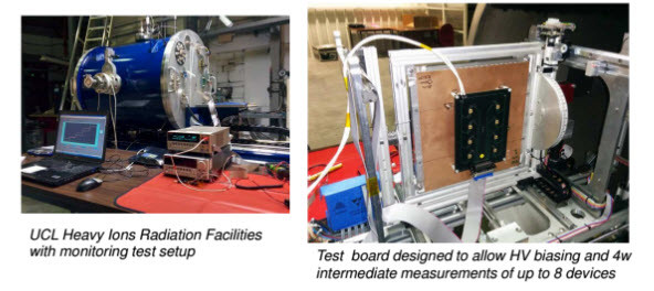
Only a PIGS (Post Irradiation Gate Stress) test reveals the cumulative damage caused by the ions reducing the voltage withstanding capability of the gate oxide. A different problem appears while testing SiC Schottky diodes where combination of high voltage and heavy ions leads to cumulative irreversible degradation.
New testing strategies need to be applied in order to detect and try to understand these new failure modes.
This better understanding starts from detecting the critical parameters involved and try to define safe operating conditions that would allow the space usage of SiC power devices.
Speaker:
Juan Moreno obtained his Bachelor Degree in Physics at the Universidad Complutense of Madrid. He has been responsible at Alter Technology of the screening and qualification of the BepiColombo and Solar Orbiter solar array SiC Schottky blocking diodes as well as technical responsible for MOS and JFET SiC transistors evaluation. Currently, he is responsible of SiC HV SiC diodes and radiation hardened MOS structures evaluation.
How approach a heavy ions test using SiC power devices – Radiation Testing
Phase 1: Allocation of critical Reverse Voltage for each LET
Dramatic failures resulting in damaged devices but…

Phase 2: Degradation characterization
Bias levels adjusted using info collected during phase 1
- Progressive degradation of the device is observed
- This allows evaluation of the Irev increase ratio Vs:
• Bias Voltage
• Flux of the beam
Phase 3: Safe Operation Range definition
Bias levels adjusted using info collected during phases 1 & 2
- Allocate maximum voltage with no degradation for a certain LET level of interest. Lower LETs than that will imply higher secure maximum voltages.
- Maximum rated voltage for this device is 1200V but under heavy ions radiation… only 250V or less is safe.
Conclusions
SiC MOSFET under heavy ions radiation:
- Only latent SEGR was observed in this study:
-> Higher Vgs during irradiation shall be used to observe in-test SEGR. - No SEB was observed in this study but bibliography points that should be observed:
-> Higher Vds biasing is needed and HV precautions shall be taken (i.e. parylene coating)
Ongoing project: Radiation Hardening of SiC MOS:
- Different gate geometries
- Different oxide types
- Several Vgs will be used to observe in-test SEGR
->Output will be an improved gate geometry + optimized gate oxide (taking also into account TID results…)
Download or read the full report here and check all the executions for the different phases
- Quantum Key Distribution - 7th November 2022
- Conducted Immunity - 20th May 2019
- Electrical transients Test - 2nd May 2019