Talk summary:
Laser beam brings unique capabilities for radiation hardness evaluation and testing of electronic components and systems. The presentation describes various laser techniques and approaches for radiation effects testing and research used in Russia by NRNU MEPhI and SPELS: SEE sensitivity parameter estimation and confirmation, IC chip de-capsulation and identification, etc. The brief compendium of laser tests during last years is also provided.
![]()

Laser techniques for radiation hardness evaluation and testing
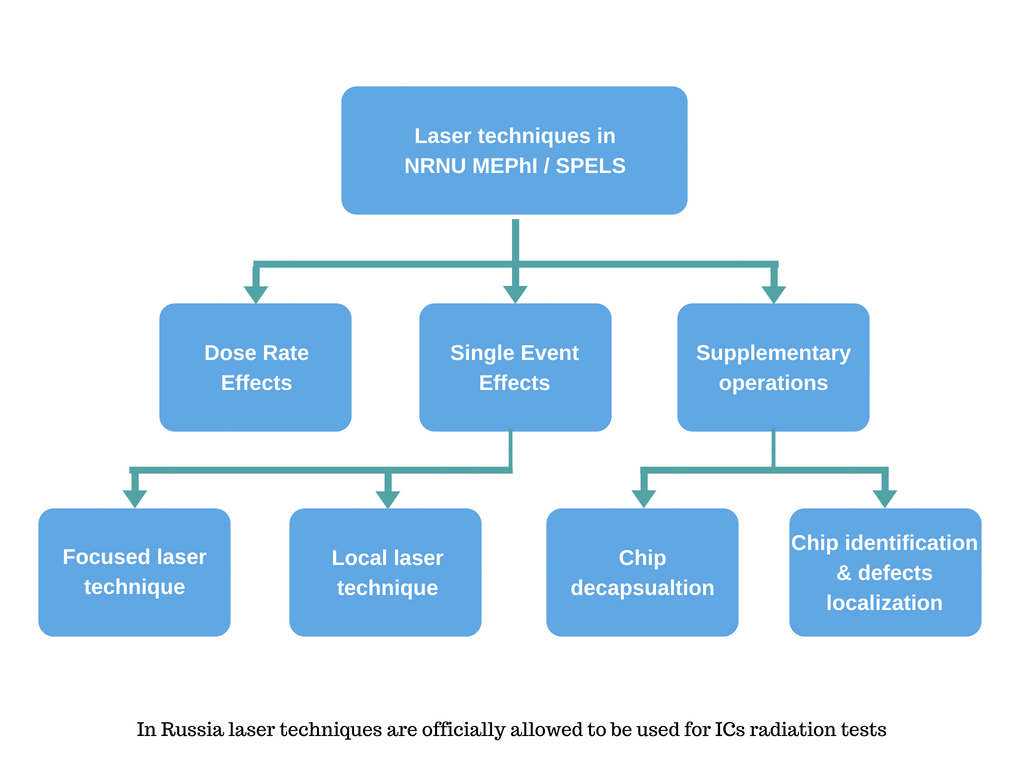
Single event effects
SEE is a serious limitation for the reliability of electronic components, circuits, and systems for space applications SEEs can be simulated by focused ultra-short pulsed laser beam
Advantages:
- Lower price
- Easy to implement
- Testing of separate IC elements
Disadvantages:
- Can’t pass through metal layers
- Does not ionize dielectric layers
- Can’t be focused to nanosize spot
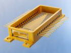
Sample preparation
It is possible to use laser for IC chip decapsulation and preparation:
- metal cover removal
- ceramic or plastic package removal
- substrate thinning (for back-side irradiation)

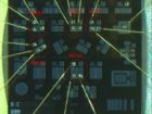
Chip identification

Focused laser facilities: the role and place in SEE research and testing
- Debugging of testing procedures and equipment;
- Ion and laser SEE cross section curves correlation;
- Testing of flip chip ICs;
- SEE sensitive nodes mapping;
- Volt-Ampere characterization of parasitic p-n-p-n structures;
- SEL “Survival” test of ICs;
- Performance check of SEE protection systems;
- SEE test at different temperatures, electric modes, etc.
SEE laser tests principles
- Laser can produce almost all types of SEEs.
- Two main mechanisms of charge generation:
− single photon absorpFon;
− two photon absorption. - Spatial distributions of generated charge by laser and ions differ, but the electrical effects are practically the same.
Download or read the full report here
- Quantum Key Distribution - 7th November 2022
- Conducted Immunity - 20th May 2019
- Electrical transients Test - 2nd May 2019