The procurement, evaluation, screening and lot acceptance of RF devices in leadless SMD packages to be used in spacecraft applications show unexpected difficulties whenever degolding or retinning processes are required. This is associated to the induced lack of coplanarity in the contacts after those.

Space product assurance (ECSS-Q-ST-60-13C) requires pure tin contacts to be retinned. Additionally, the assem bly processes selected by the OEMs requires gold finish to be removed and replaced by tin-lead alloys.

External views of the sample

This task has been systematically considered simple but hides a big problem: it is not possible to make the pads perfectly flat and co-planar post dipping. This is a solder dip process so that this is a result of the surface tension of the solder and the geometry of the pad.
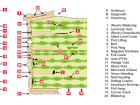
External views
- De-golded and pretinned sample
- Orientation Pin Marker
- Copper Via Metallizations
External views
- De-golded and pretinned sample
- Orientation Pin Marker
- Copper Multilayer
- Stripline
- Contacts
External views
- Orientation Pin Marker
- Ports
- GND
- Unbalanced
Typically, after degolding or retinning processes, solder thickness not to exceed 0.002 inches, so maximum non-planarity would as small as such 0.002 inches. However, this small non-planarity in the pads of a component produces poor or inexistent electrical contact between the test fixture and the device.
This results in parasitic effects that distort the electrical measurement at microwave frequencies. When a small air gap is present between the signal pad and the test fixture, its effect may be modeled mainly as a series capacitance and a resistance.
Its effect may behave as a high-pass filter with uncontrolled cut off frequency, ant it can also produce reflection of the input signal due to mismatched input impedance.
The same can occur in a ground pad that affects the grounding of the device converting it in a floating ground or reference.

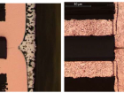
Results of a device that has undergone the degolding + pretinning processes and failed the subsequent electrical measurement.
There are methods for levelling the solder after, but screening activities for space applications require extreme care during the manipulation of the EEE parts to be assembled on a spacecraft, and those all carry a high risk of damage to the package.
Alter Technology has defined a procedure for the degolding / retinning processes by optimizing the parameters involved for each component (time and temperature in solder baths, for example), defining cleaning actions on contacts before and after and using a specific method of evening without damaging the devices.
A customized test fixture specifically designed for the electrical measurements is also developed, as necessary. Both together minimize or avoid the negative effects described above and avoid false rejection of functional parts.

Results of a device that has undergone the degolding + pretinning processes and passed the subsequent electrical measurement. These are similar to which can be obtained on a sample not subject to any previous process.
Authors: Dimas J. Morilla, Aintzane Lujambio, David Nuñez Teruel, Manuel Domínguez.

She joined Alter Technology Tüv Nord in 2017 as development engineer for microwave components. With an experience of more than 10 years in the microwaves industry, she is working at the EEE parts laboratory department as head of the Microwave Laboratory. She has been involved in testing activities such as screening and qualification of microwave components for different space missions such as ESA’s JUICE mission.
She also represents Alter Technology Tüv Nord within the Microwave and RF Passive working groups of the Components Technology Board (CTB), the board responsible for the formulation of strategic programs and work plans for technology research and development in the area of European EEE space components.
- Balanced-to-Balanced Microstrip Diplexer Based on Magnetically Coupled Resonators - 4th April 2018
- Degolding and Retinning Processes On Leadless SMD Packaged Devices - 16th February 2018
- Compact Balanced-to-Balanced Diplexer - 15th February 2018