Solder bumps versus Au bumps
SAC305 solder has been included as a Bump Technology, as this tends to be the most common solder bump material. However, other common solder bump options such as SnPb, have similar thermal, electrical and mechanical properties. Table 5 below provides a summary of the thermal, mechanical and electrical comparison of solder bump and Au bumps.
Table 5: Comparison of the mechanical, thermal and electrical parameters of different bump technologies.
| wdt_ID | Process | CTE (ppm/oC) | Scale | Dimensions (µm) Diameter | Dimensions (µm) Height | Elec. Resistance (µΩ/m) | Thermal Conductivity (W m-1 K-1 ) | Tensile strength (mPa) | Hardness (Vickers) |
|---|---|---|---|---|---|---|---|---|---|
| 1 | Au stud Bumps | 14.4 | Die or Wafer | 50 - 90 | 35 - 50 | 0.0220 | 320 | 220 | 216 |
| 2 | SAC305 Bumps | 27 | Wafer | 60 - 70 | 50 - 75 | 0.13 | 58.7 | 29.7 | 14 |
| 3 | Electroplated Au Bumps | 14.4 | Wafer | -- | 17 - 25 | 0.0220 | 320 | -- | 123 |
| Process | CTE (ppm/oC) | Scale | Dimensions (µm) Diameter | Dimensions (µm) Height | Elec. Resistance (µΩ/m) | Thermal Conductivity (W m-1 K-1 ) | Tensile strength (mPa) | Hardness (Vickers) |
Please note that we have not considered Cu pillar bump technology in this analysis due to the small amount of reliability data on this technology for Space applications and the relative immaturity of the technology.
The key conclusions from Table 5 are given below;
- Au bumps, either electroplated or Au stud bumps, have a closer CTE match to GaAs and Aumina compared with SAC305 solder bumps.
- The electrical resistance of the Au bumps, either electroplated or Au stud bumps, is lower than with Solder bumps and hence provides better current carrying capacity and electrical performance.
- The thermal conductivity of Au bumps, either electroplated or Au stud bumps, is over 5 times higher than with SAC305 solder bumps. This aid the heat dissipation from the MMIC device into the substrate.
- Height – the bump will compress up to 50% during the flip chip attach process. By using a harder Au material for the stud bumps then the compression can be reduced which limits the stand-off distance. Such an option is not available for solder bumps.
- Tensile strength and hardness – The lower tensile strength of solder bumps means the solder bumps will have more stress relief. This is one advantage of solder over Au bumps.
In addition to the electrical, thermal and mechanical benefits listed above, Au stud bumping, in particular, has a number of other advantages over solder bumping.
- Au stud bumping can be performed on both the die and wafer level providing more flexibility and reducing costs.
- Au Stud bumping also offers the potential for a flux free flip attach process, unlike solder bumps, which typically require flux. The flux can have a negative impact on the reliability and electrical performance MMIC devices.
- Au stud bumping does not require any under bump metallisation (UBM) layers. As long as a bond pad is suitable for Au ball wire bonding then it can be Au stud bumped, whereas solder bumps require UBM layers to ensure that the solder bumps can adhere to the bond pads and to avoid diffusion of metals into the MMIC device.
Au Stud Bumpin
Au stud bumping is a technique for creating conductive gold bumps on a die bond pad which ultimately enable the die to be electrically interconnected to a package or substrate through an adhesive, thermo-compression or thermo-sonic flip chip attach process.
Au stud bumping uses a modified wire bond process, whereby the Au ball is formed on the die bond pad, as in wire bonding, but instead of spooling the wire to a package or substrate, the wire is cut just above the ball to leave a stud bump on the die bond pad.
See Figures below for more detail on Au stud bump formation;
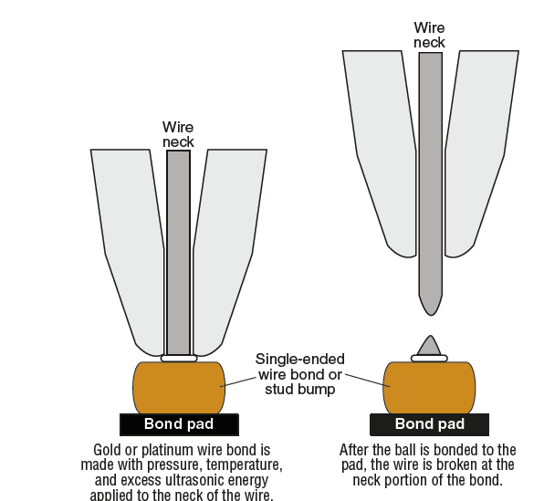
Figure 8: Au stud bump formation
The advantages of Au stud bumping have been described above. One of the key benefits is the ability to easily vary the bump dimensions which in turn
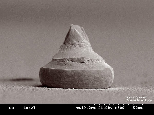
Figure 9: traditional bump shape with no flattening of bump
Diameter: 80um
Height: 55um
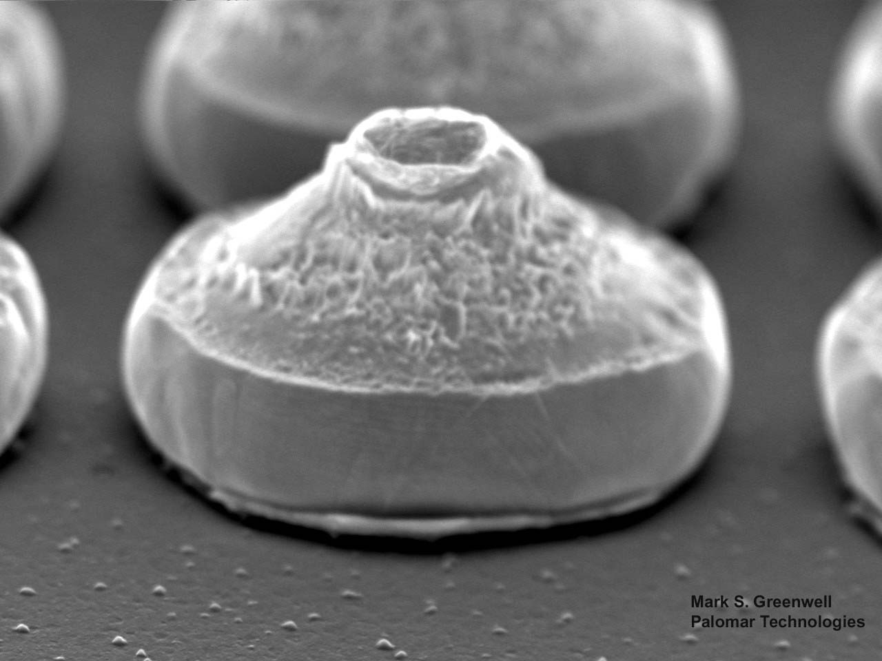
Figure 10: bump using shearing feature on wire bonder
Diameter: 70um
Height: 20um
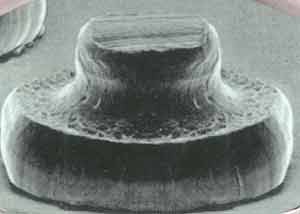
Figure 11: bump after coining process
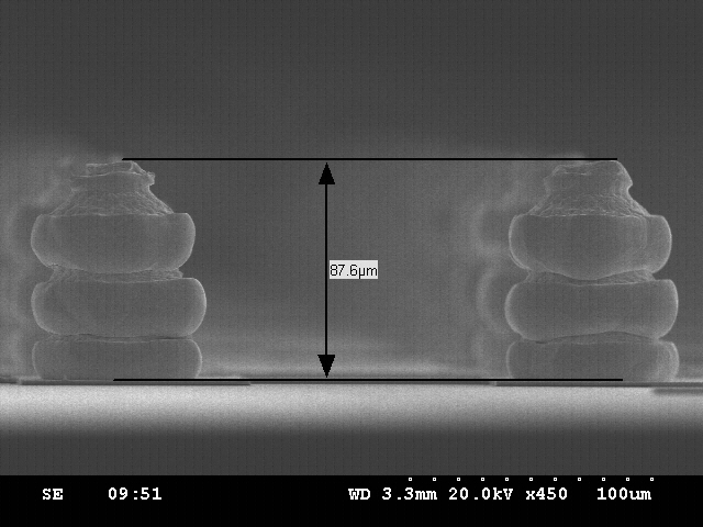
Figure 12: stacked bumps
As previously discussed the bump dimension can have an important impact on reliability and electrical performance. However, the bump shape can also have an impact on the chosen flip chip attach process.
The bump shown in Figure 10 differs from the typical bump of Figure 9 in not having the wire tail or pointy peak. This bump is designed specifically for flip chip assembly using either a thermo-compression or a thermo-sonic assembly process. The bumps in Figure 10 show a softer, blunter peak than the Figure 9 bump. This shape will help direct the compression forces to assist in the formation of an inter-metallic bond at the second surface. By focusing the applied energy onto a smaller surface area, the other bonding factors (heat, force and ultrasonic energy) can be reduced. As this bump continues to be compressed during assembly, the surface area in contact with the substrate pad will grow, increasing the conductive area.
A ball bump shape like the one in Figure 11 may be preferred for isotropic conductive epoxy assembly. This bump has a centre stud, with a flat surface finish on the upper surface of the bump. The flat finish was created by a coining process which involves a flat tool compressing the top of the bump. This flat finish provides a better surface for conductive epoxy to adhere to, and to remain in place during the flip and attach assembly steps.
The bump configuration in Figure 12 shows a number of Au stud bumps stacked on top of each other. This configuration is sometimes used in applications requiring a large stand-off distance.
Reliability of Au stud bumps
Due to the Au bond pads on most MMIC/RF die then we are able to create a mono-metallic interconnection with the Au stud bump. This is a positive design consideration from a reliability perspective. For example, most Silicon based semiconductor devices have Al bond pads and at high temperatures, either during the subsequent flip chip attachment or during operation, there can be formation of Au-Al inter-metallic’s which will impact the joint integrity and reliability.
The use of Au stud bumps on MMIC devices in Space applications is already reported in the following paper S. George, C.Drevon, JL Cazaux “Flip Chip for space applications: Bonding reliability, DC and RF results”
Substrate
The table below to download, provides a summary of the typical substrates used for MMIC assembly from an electrical, mechanical and thermal perspective.
Substrate – CTE
One of the major reliability issues for flip chip interconnect joints is stress due to thermal/power cycles. The fatigue stress originates mainly from the Co-efficient of Thermal Expansion (CTE) mis-match between then die and the substrate material. Looking again at equation (1)
It can be seen that minimising the CTE difference () will minimise the stress of the bump connections and hence improve the reliability. Typically for most semiconductor devices an underfill is used to provide stress relief between the die and substrate and re-distribute the stress over the entire plan and hence minimise stress of the joints furthest from the centre. However, as we will discuss later, the underfill may have a deleterious impact on the electrical performance in the millimetre-wave frequency range. As a result it is even more important that we have good CTE matching between the die and substrate. The CTE of GaAs is 5.7ppm/°C. Looking at Table 6 it can be seen that the best material from CTE matching perspective is Alumina.
- Quantum Key Distribution - 7th November 2022
- Conducted Immunity - 20th May 2019
- Electrical transients Test - 2nd May 2019