Factors influencing selection of bump technology
A number of options exist for bumping a semiconductor device including solder bumping, Au bumps and Cu pillar bumps.
When selecting the optimal bump material to use a number of factors must be taken into consideration. These factors are listed below;
- Melting or Weld temperature of bump
- To ensure a controlled solder hierarchy is achieved and that the part is manufacturable.
- To ensure the attachment temperature does not exceed the limit of the MMIC die operation.
- To reduce the zero-stress temperature and improve reliability.
- Stand-off distance
The separation/stand-off distance between the MMIC die and the substrate is determined by the bump height and the subsequent bump height compression during the flip chip process. This stand-off distance has an important impact on the high frequency electrical performance in terms of the coupling effects between the MMIC and substrate. The stand-off distance also has an important impact on the stress relief and the corresponding assembly reliability.
It should be noted that the smaller the bond pad then the lower the bump height and hence the smaller the stand-off.
For example the shear strain on a bump connection in a flip chip assembly is given by the following equation (1) below;
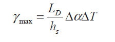 where hs is height of the solder joint, is CTE difference, T is the temperature difference between cold cycle and hot cycles, and LD is half of the diagonal length of the die.
As can be seen the stress and hence reliability of the connection is determined by a number of factors, all of which will be discussed later, but the larger the stand-off then the shear strength is less and hence is better from a reliability perspective. The greater the standoff the more like original performance will be. Too great a standoff may introduce modes for stray signals to propagate. See Figure 2d.
- Pad and Bump Geometry
There are limitations in the dimensions of different bump materials and the bump dimension should be closely matched to the bond pad of the MMIC die and the bond pad of the substrate. If these dimensions are closely matched then stress of the connection will be equally spread out. However, for example, if the bump is larger than the die bond pad then there could be excessive stress on this bond pad which could lead to a weakness and ultimately a reliability concern.
- Co-efficient of Thermal Expansion (CTE)
To provide as close a match as possible for the bump, die and substrate CTE to minimise any stress. As can be seen from Equation (1) the smaller the then the smaller the shear strain on the bumps.
- Thermal Conductivity
This should be as high as possible to help disperse heat generated by die operation and current flow through the interconnects.
- Tensile strength and hardness
This needs to be balanced to optimise the bump’s ability to both absorb strain and transmit strain throughout the package to minimise the likelihood of bumps fracturing.
- Quantum Key Distribution - 7th November 2022
- Conducted Immunity - 20th May 2019
- Electrical transients Test - 2nd May 2019