Laser Diode Packaging and Fiber Alignment
The purpose of packaging for a laser diode is four-fold.
Firstly, it provides electrical interconnection for the laser diodes, photodiodes, thermo-electric coolers, and any other components, to the outside world.
Secondly, it provides an optimized platform to dissipate the heat generated from the laser diode, and any other internal component, and ensure that the optical device operates optimally. In situations where the thermal resistance of a package is too high then laser diodes will roll-over after a certain drive current and the maximum optical output power will not be achieved.
Thirdly, it provides mechanical support and environmental protection for sensitive and delicate laser devices. The lifetime of laser diodes is very sensitive to the environment that it sees. Excessive water absorption or the presence of organics on the facets of laser diode can result in significant degradation of the lifetime. Co-efficient of Thermal Expansion matching between the laser device and the submounts on which they are bonded are very important to ensure that there is no mechanical damage or stress induced into the device.
Lastly, the package provides a convenient means for coupling the light from a laser diode to the outside, usually by means of an optical fiber or sometimes windows and optics.
Selection of the right package and assembly process is critical in meeting the performance, reliability and cost targets of laser modules. The following sections will review the key design, material and process considerations for packaging of laser diode and other optical devices.
In Optocap’s case we already have a space qualified PM fiber coupled, 14-pin butterfly package.
Design
A good understanding of the optical design is key to optimal package design and selection of the optimal assembly process. For example, selecting a low tolerance component attach process, such as adhesive, for a process that requires high positional tolerance, such as a single mode fiber, will result in performance and reliability issues.
The use of optical modeling software during the design phase will allows Optocap to determine the sensitivity of the laser diode and fiber assembly positional placements on the associated coupling efficiency. Sub-micron manipulation of the fiber assembly is usually required to achieve suitable coupling efficiencies. A high coupling efficiency enables the laser chip itself to be de-rated which in turn offers the opportunity to further increase the chip lifetime.
In addition, a suitable fiber attach process that can maintain sub-micron placement after attachment will be required to maintain high coupling efficiency for the lifetime of the module. In this respect Optocap use a Telcordia and space-qualified and well understood laser weld attach process.
Thermo-mechanical finite element modeling (FEM) is used at the front end of any package design to assess the mechanical design positional stability and component temperature gradients over package temperature exposures and device thermal loading. Mechanical stability and robustness of sub mounts and attached components is necessary to maintain optical alignment and device performance under thermal loads of elevated package temperature, environment, TEC operation, and laser diode operation. Design solutions to these thermo-mechanical packaging issues include: choice of sub mount thickness for resistance to thermal gradient warpage; proper TEC sizing; material selection of sub mounts for thermal conduction; and sub mount ability to provide temperature uniformity across its surfaces.
Optocap have a good handle on all these material selections issues and trade-offs and typically mount laser chips on sub mount onto a Kovar optical bench. Kovar optical benches are used for our space qualified 14-pin butterfly package. The benefit of using the Kovar bench is that it acts as a heat-spreader, meaning that it takes the localized heat from the laser chip on sub mount and spreads it across the much larger optical bench. This heat-spreading ensures that the full area of the TEC is used and ensures that the TEC operates optimally. Note: the Kovar optical bench allows thermal co-efficient expansion matching with the laser weld clip and TEC. The laser chip should be mounted to the sub-mount using a hard-solder, such as AuSn, this avoids any creeping of the solder joint and ensures that the alignment of the laser to the fiber is not impacted.
Component Attach
A number of components, including TEC, optical bench, thermistor, and photodiode will need to be optimal attached to ensure the module performance and reliability is achieved. For example, non-optimal attach of a TEC, due to voids in the solder joint interface, can severely impact the thermal performance and non-optimal attach of an optical bench can lead to shifts in fiber alignment and impact the optical coupling. The following paragraphs describe the variables that must be considered for optimal component attachment in a laser diode module.
The key component attach methods are based on either epoxy or solder approaches.
While epoxy attachment is generally considered the lowest cost entry attachment process for building photonic devices, it is commonly used in photonic device proof-of-concept demonstration builds and early prototype builds because of its ease of use, low cost, availability and the absence of reliability requirements. However, concerns over outgassing properties and mechanical stability mean that Optocap would not consider an epoxy attach process suitable space qualified modules. Material outgassing is particularly a concern for laser transmitters and laser pump modules. Outgassing effects include degradation of optical coupling by condensation on optical surfaces and degradation of reflection coatings at high optical densities on laser facets.
Optocap’s laser modules are based on an all solder construction. It is worth noting that this does not apply to the attachment of the fiber assembly, which as discussed previously, is attached using a qualified laser weld process.
Solder is an excellent method for mechanical attachment of sub mounts and components, especially for designs that require high thermal conduction through the sub mounts. The use of flux in the soldering process requires special attention in the manufacture of photonic devices due to reliability concerns from flux contamination.
Single Mode Fiber Attach
Laser welding is a process that can deliver highly repeatable submicrometer attachment in a production environment, assuming the weld-attachment processes are well understood and if the device is designed for laser-weld manufacturability. Optocap have several years experience of the laser weld process and have assembled thousands of such modules in our facility with this process. The key areas of laser weld process knowledge to be aware of are; materials selection, joint tolerances, laser weld set-up, post-weld-shift (PWS) repeatability and PWS correction and weld clip design.
The ability of laser welding to join optoelectronic components with repeatable submicron precision distinguishes it from other forms of attachment technologies, including laser soldering, ultraviolet-cured epoxy, and thermally cured epoxy. The need for submicron precision arises from the requirement to efficiently couple single-mode fibers, waveguides, or modulators.
Process yield and repeatability have often dictated the use of laser welding in the manufacture of laser modules. Typical attachment tolerances can be 250 nm, with alignment requiring optical beam-profiling step sizes of 50 nm. This level of precision generally precludes the use of epoxy and soldering attachment due to difficulty in achieving repeatability at submicron tolerance in a manufacturing environment.
Attaining this level of precision with laser welding demands substantial processing, materials, and welding knowledge. All processes require active alignment, typically using optical power monitoring.
The weld schedule and pattern is important to produce minimal, repeatable shift and to address any thermal heating issues. Cross-section analysis of the weld joint is performed as a quality assurance measure.
Polarization Maintaining (PM) Fiber Alignment
Polarisation maintaining fibre-optic modules requires specialised fibre and connectors and careful assembly as well as alignment to achieve optical performances, which are affected by the polarisation of the light travelling through the fibre. To solve the problem of polarisation-dependent losses, several manufacturers have developed polarisation-maintaining fibres (PM fibres). These fibres work by inducing a birefringence within the fibre core. Birefringence is created within a PM fibre either by forming a non-circular fibre core (shape induced birefringence), or by inducing constant stresses within the fibre with stress applying parts (SAP) (stress induced birefringence). This birefringence breaks the circular symmetry in an optical fibre, creating two principal transmission axes within the fibre, known respectively as the fast and slow axes of the fibre.
At present the most popular fibre type in the industry is the circular SAP type (stress induced birefringence), or PANDA fibre. One advantage of PANDA fibre over most other fibre types is that the fibre core size and numerical aperture is compatible with regular single mode fibre, ensuring minimum losses in devices using both types of fibres.
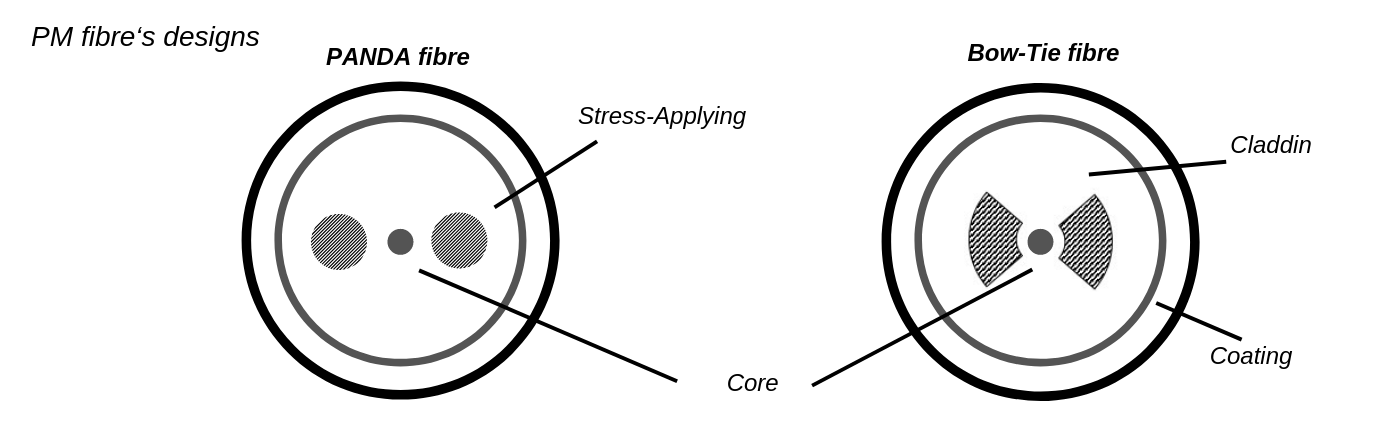
Different PM fiber designs.
Provided the input light into a PM fibre is linearly polarised and orientated along one of these two axis, then the output light from the fibre will remain linearly polarised and aligned with the principal axis, even when subjected to external stresses.
While in theory one can produce perfectly linearly polarised light, in practice this is not the case. Instead there is always some residual polarisation, random or elliptical, present in the output light. To measure the quality of the polarised beam, one must measure its polarisation extinction ratio (ER).
Naturally, how well a fibre maintains polarisation depends on the input launch conditions into the fibre. Perhaps the most important factor is the angular alignment between the polarisation axis of the light with the slow axis of the fibre. Assume that we have a perfectly polarised input beam into an ideal fibre, misaligned by an angle f with respect to the slow axis of the fibre. Because of this misalignment, a small amount of light will be transmitted along the fast axis of the fibre. This will degrade the ER of the output beam. The maximum possible value of the output extinction ratio is thus limited by:
EXTINCTION RATIO (ER) £ 10 log (tan2f)
Thus to achieve output extinction ratios greater than 20dB, the angular misalignment must be less than 6 degrees. For 30dB extinction ratios, the angular misalignment must be less than 1.8 degrees.
PM fibre products show a highly delicate nature due to the sensitivity of PM fibre to stress. Stress in the fibre modifies the birefringence and reduces the ER value, which is the parameter that describes the efficiency of polarization maintaining. Connectors usually stress the tip of the fibre and reduce its ER.
- Quantum Key Distribution - 7th November 2022
- Conducted Immunity - 20th May 2019
- Electrical transients Test - 2nd May 2019