Materials and Processes laboratory combines accurate characterisation techniques and inspection tools with deep scientific and technological background in materials science. The mission of this area is to thoroughly assess the reliability of materials and processes involved in the manufacturing of spacecraft components.
Materials and Processes task involves three types of interrelated activities.
PCB and soldering verification
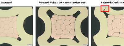
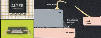
PCB assembly of SMD devices and soldering operations remain amongst the more delicate space-componentsfabrication task as they may compromise the integrity and performance of the whole system. These processes requires specifically trained and skilled operators. Hence ESA pays special attention to the workmanship assessment and have issued specific regulations concerning this issues, ECSS-Q-ST-70-08C and ECSS-Q-ST-70-38C, some of them recently updated.
Alter Technology Material and Processes area conducts full soldering and SMD verification test-programmes according to the ESCC specifications. For this purpose, our facilities include a full equipped laboratory to carry out microsectioning inspection together with an environmental laboratory to perform the temperature and vibration test required for PCB and SMD verifications. The facilities and the involved stuff are about to complete the process to become an ESA recommended laboratory to perform these evaluations.
Materials Analysis
Elemental chemical analyses provide accurate information about the elemental chemical composition of the inspected materials. They are a critical in different Hi-REL- verification programmes to assess the compliance with the international regulations (e.g. MIL-DTL detail specifications of the USA Defense and Logistic Agency (DLA), ASTM international, NIST standards as well as ESCC regulations of the European Space Agency).
Therefore, they are routinely used to:
- Verify that the inspected material fulfils the required compositional specifications.
- Discard the presence of prohibited elements and trace-element contamination, corrosion (oxidation) and others.
On the other hand, fine elemental analysis together with advanced microscopy techniques play a critical role in failure analyses to ascertain and understand the root cause and prevent future fails.
Alter Technology compositional-analyses capabilities cover most of the international regulation requirements and are adapted to the customer needs in term of:
- Analyses volume: Bulk, surface or depth profiling analyses.
- Destructive or non-destructive character and sample preparation.
- Sensitivity/cost balance: From major components identification to trace-elements quantification.
Microscopy
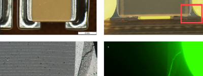
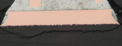
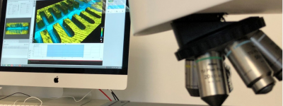
The microscopy facilities available at Alter Technology are perfectly adapted to conduct either conventional inspection task as well as fine analyses requiring advanced instruments. Amongst others, it is worth remaking the FIB capability to perform accurate SEM microsection inspections on semiconductor systems.
Equipment and main technical capabilities:
- Focused Ion Beam (FIB) + Electron Microscopy (SEM) for serial nano-sectioning.
- Non-destructive internal inspection by C-mode Scanning Acoustic Microscopy (C-SAM).
- 3D Radiographic tomography and virtual micro-sectioning.
- Bulk (X-ray fluorescence spectroscopy- XRF), surface (X-ray photoemission spectroscopy- XPS) and depth profiling compositional materials analyses.
- High resolution Electron Microscopy (SEM) and X-ray compositional microanalysis (EDS) normal and cross section view.
- Microsectioning + fluorescence Microscopy.
Main Test Services:
- Soldering Verification.
- Component defects evaluation.
- Raw material evaluation
- PCB coating evaluation.
- Blistering and delamination analysis.
- Tin wisker testing
- Moisture and Insulation Resistance
- Dielectric Withstanding Voltage
- Thermal Shock
- Temperature cycling.
- Thermo-mechanical failures.
- 3D Dimensional verification
- Vibration test.
VIRTUAL LAB
- Access to your test results in real-time.
- Live Chat with our inspectors
- Time Cost Saving.
Click here and enter in Virtual Lab
Full Accredited:
- ESA recommended Microsectioning Laboratory in accordance with ESA-TECMSP-MO-013165,
- ISO/IEC 17025:2017, and
- ESA certified inspectors in accordance with ESA-STR-258.
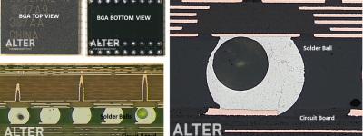
MacroVoids in assembled BGA packages
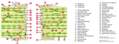
Microsection Inspection / Constructional Analysis
Soldering Verification Processes
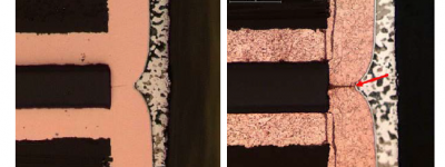
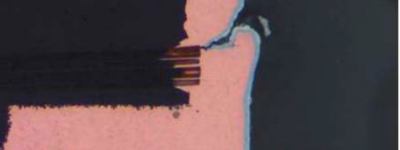
PCB Failure Analysis: Pad Cratering
Noncontact 3D Characterization Using Confocal Laser Scanning Microscopy (CLSM)
PTV Failure: Manufacturing Defects
Plated Through Via Failures
Thermomechanical Failures in Plated Through Vias (PTVs)
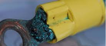
Failure Mechanics and Causes in Crimped Connectors