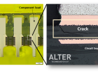
Failures in plated through vias (PTV) can be related to different causes, some of them discussed elsewhere. Amongst them, thermomechanical fatigue is the most frequent failure mechanism observed in plated through systems. Hence, the present post analyses the typical thermally induced failures in PTV architectures.
Nasa Reliability of PWB Microvias for High Density Package Assembly Body of Knowledge (BOK)
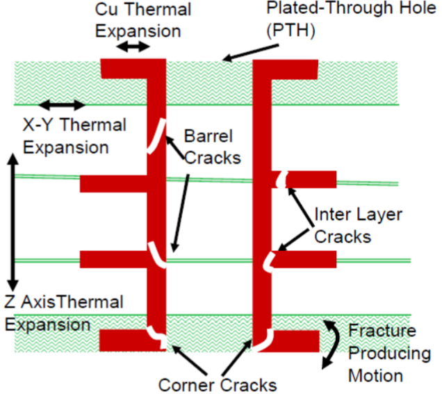
Thermomechanical stress in PCB/PWBs is generated by the mismatch between the coefficient of thermal expansion (CTE) of the materials comprising the system. In general laminate materials used for PCB fabrication, as well as other dielectric polymers, have larger CTE than metal traces/pads and the plating of the PTV. Therefore, ambient temperature changes or operational power dissipation induce cyclic stress which leads to fatigue failures.
On the other hand, PCB laminates may also exhibit large anisotropy in the CTE which generates different types of failures at the PTH, as it is described below. Such anisotropic response is due to the incorporation of reinforcement materials (e.g. glass or aramid embedded fibers) that effectively reduces the in plane (X and Y direction) CTE, but with a minimum effect on the Z-axis thermal expansion.
The figure gathers several common thermally induced failures and the locations within the PTH/PTHV architecture.
Barrel Cracks
Cracks observed at the PTV barrel after thermal cycling are due to the high CTE contrast at the Z direction between the organic resin and the copper traces. This preferential Z deformation is due to the low effect that the embedded reinforcement material has on the Z-CTE.
This failure is typically initiated at glass fibers on the inner edge of the drilled hole. Once initiated it advances through the boundary between the Cu grains and propagates into the barrel thickness.
During thermal cycle testing, below the resin glass transition temperature, such fatigue-induced-cracks propagate into the barrel of the PHT/PTV. This failure mode is frequently detected in boards after few cycles in case of a preexisting damage material; or hundreds and thousands of thermal cycles in the case of robust PCB systems.
Barrel crack generated after thermal stress
From ECSS-Q-ST-70-60C
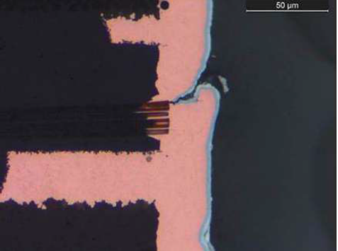
Inner-layer separation
Inner-layer separation (ILS) failures comprehend inner-layer Cu foil failure, separation of the Cu flash and electrolytic Cu, or separation of the foil and Cu flash. In contrast with barrel cracks which are due to the high Z-axis CTE mismatch, ILS is related to in plane resin expansion into the free space of the PTH. A Cu foil with good quality can preclude or significantly delay this failure mechanism. This is so because, when the Cu wall is thick enough to deform only elastically ILS is not generated. However, if the barrel wall is too thin the barrel will plastically deform leading to large tensile stress at the PTH inner contact points.
Example of Inner layer separation
2016 17th International Conference on Electronic Packaging Technology 978-1-5090-1396-8/16/$31.00 ©20161EEE
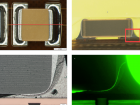
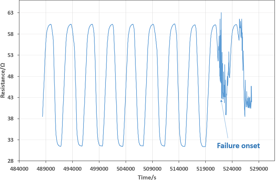
In-situ detection.
During thermal cycling, thermomechanical failures may both gradually degrade the system conductivity or even lead to sharp electrical discontinuities. Therefore, during such thermal test the daisy chain resentence of the system is continually monitored. This allow us to early detect the generation of thermally induced fails. Providing a real time information to our customers thanks to the Virtual lab platform.
Example of the detection of thermomechanical failures during a thermal cycling test conducted in Alter Technology
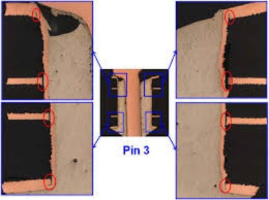
Cross-section inspection.
As indicated in the text, fail location is a clear indication of the CTE mismatch causing the electrical failure observed by in situ electrical monitoring. Such a failure analysis requires of internal microsection inspection of the passing through via.
Micro-sectioning is a delicate destructive process whereby the PCB area under inspection or a test coupon is precisely excised from the system to be mounted in an epoxy resin. Afterwards the sample is ground and polished according to the system characteristics in order to reveal the true internal structure. This is a complex task involving different preparation steps adapted to the sample characteristics that require highly trained staff, to avoid preparation induced anomalies.
In contrast with to other labs in Alter Technology combine micro section inspection with fluorescence microscopy techniques, which has been proved to be an effective approach to avoid false rejections and to highlight small anomalies.
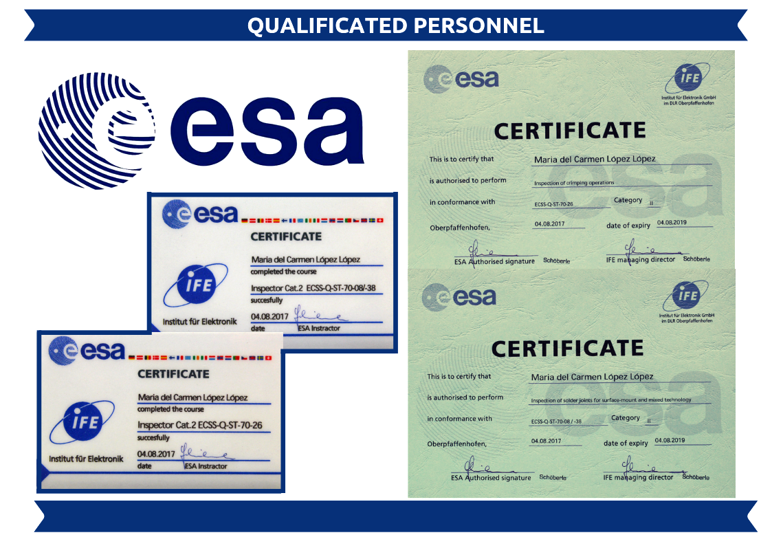
In Alter Technology micro-sectioning is accomplished in a specifically dedicated laboratory and by ESA certified staff on PCB/SMD inspection. ESA selects those laboratories that according to the higher quality standards are recommended to perform such operations on SMT/PCB systems. It is worth mentioning here that due to the high-level standard that Alter Technology maintains in all its activities it is currently an ESA recommended laboratory to conduct metallographic inspections in SMT systems.
Contact us for more information

Since 2007 Dr Aparicio has developed a productive research career within the field of Materials Science including post-doctoral stays at the University of Trento, the University of Mons, and the Spanish National Research Council (CSIC). His researches have been published in more than 30 articles in reputed international research journals and conferences (> 70) including more than 10 invited talks and lectures.
Within the frame of the programme “Torres Quevedo” for the Knowledge Transfer and the incorporation of research talent into the industry, in 2019 he joined Alter Technology as Senior Materials Science Test Engineer. In 2019 he was appointed to lead the Scanning Acoustic Microscopy Service. Within this framework, he currently collaborates in different ESA projects (JUICE and PLATO).”
- Scanning Acoustic Microscopy on Ceramic Capacitors - 18th May 2020
- Non-destructive detection of micrometric internal features within EEE microelectronic systems. - 3rd September 2019
- Acoustic Inspection of Hybrid Systems on Laminated Substrates - 3rd September 2019