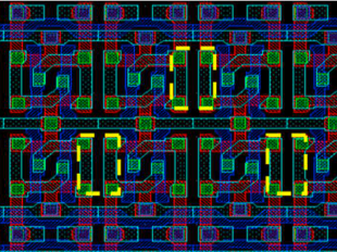
Third party dice radiation test for a manufacturer has never been an easy thing thanks to the exigent requirement from the users and difficulties from the die side. Things are becoming worse since the semiconductor came into a sub-micron and deep sub-micron era. New challenges...
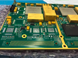
VA160 and VATA160 are used as front-end readout ASICs in the payloads of DAMPE. Both Laser pulse test and heavy ion beam test were conducted to get the SEL tolerance of the ASICs. Laser test was performed firstly to quality the SEL sensitivity because it is easy and ready at all...
Laser beam brings unique capabilities for radiation hardness evaluation and testing of electronic components and systems. The presentation describes various laser techniques and approaches for radiation effects testing and research used in Russia by NRNU MEPhI and SPELS: SEE...
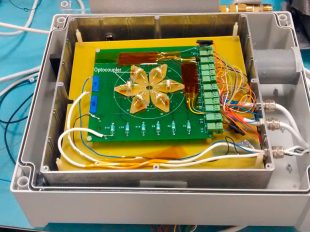
A modular architecture specifically designed for integrating technology demonstrators and test applications in a fast-to-orbit cycle allows any interested team to prepare its payload for flight into orbit in less than 1 year. Existing radiation models and continuous monitoring...
In order to evaluated the displacement damage on device induced by energetic particles in space, various device samples including optocouplers, solar cells, and bipolardisplacement damage radiation testing ransistors are irradiated with protons, neutrons and γ-rays. The...
Electronics systems designed for applications in high radiation environments, such as space missions, high energy accelerators and avionics, are subject to a radiation qualification process at component level which is often time consuming and expensive. The new CERN High energy...
Goal of the study • Propose a DD test standard • Should be available by the end of the year after ESA and Components Technology Board (CTB)/Radiation Working group (RWG) comments • Goal of this presentation ⇒ Not a draft of the future guidelines, but: • Remind the physical...
Radiation assurance test is very interesting, but also very complicated. It always needs joint efforts to find better solutions, and BMTI is looking forward to collaborating with related partners to do this.

New failure modes not observed in Silicon appear while testing SiC MOSFET and Schottky diodes and under heavy ions radiation. Gate damage in transistors remains undetected even monitoring drain current and gate leakage of the transistor under high voltage biasing conditions.
En aplicaciones espaciales, los optoacopladores pueden necesitar trabajar a temperaturas muy bajas. Bajo estas condiciones de operación a baja temperatura, la degradación del dispositivo sometida a exposición a la radiación puede mostrar un comportamiento diferente en...