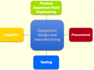
The activity of product assurance (PA) support performed by Alter technology engineers is being more and more demanded and appreciated by space customers due to the high level of mastering required on components technology knowledge, space requirement/environment understanding... Continue reading
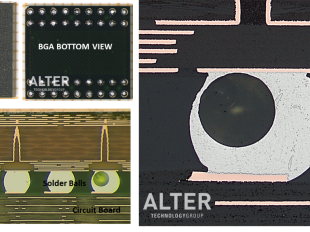
BGA device assembled to a PCB has been submitted to the ECSS verification programme following the guideline defined in the ECSS standard ECSS-Q-ST-70-38C. Continue reading
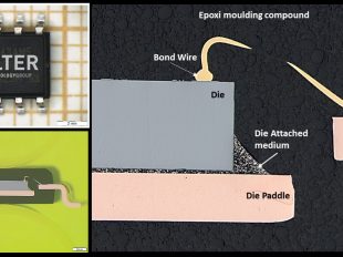
Cross-section analysis is a very useful way of determining the construction and material composition of electronic devices. The FP device is potted in epoxy resin. After curing, the sample is sequentially grinded up to reach the plane of interest. Then, the specimen is subjected... Continue reading
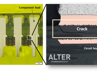
Microsection analysis is performed on an assembled through-hole device as a part of failure analysis. Cross-section through the plane of interest can provide helpful information about solder defects, PCB inner layers, and internal construction. As a part of failure analysis, the... Continue reading
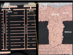
The separation of the interest area has to be performed in such a way as to prevent any damage by deformation or input of heat. After cleaning, the specimen is encapsulated before the grinding process takes place. Continue reading
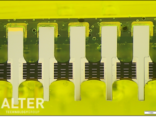
Assembly process of THT or SMT onto PCBs for spacecraft applications follow well-established design requirements based on specifications prepared by ECSS (ECSS-Q-ST-70-08C & ECSS-Q-ST-70-38C), NASA and IPC (IPC-6012). Continue reading
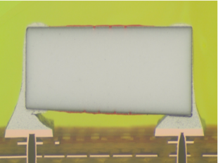
Resistors assembled to a PCB have been submitted to the ECSS verification program. Metallographic analysis allows us to check the status of such devices after performing the environmental tests (Vibration & Thermal Cycling). Continue reading
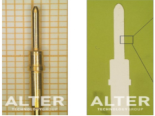
Cross-sectioned pins were metallographic prepared in ALTER TECHNOLOGY Materials & Processes Laboratory, recognized as a recommended facility for such activity by ESA authority (MEMO ESA-TECMSP-MO-013165). Continue reading
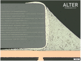
Cross-sectioned ceramic capacitors were metallographically prepared in the Materials & Processes Laboratory, recognized as a recommended facility for such activity by the ESA authority (MEMO ESA-TECMSP-MO-013165). Continue reading
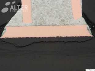
Pad Cratering One of the major failure modes encountered in PCB assembly is Pad cratering. This term is coined to describe a fracture at the pad/resin interface (adhesive failure) or within the resin beneath pads (cohesive failure) that extend along the whole pad length (see the... Continue reading
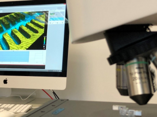
At Alter Technology, we can perform 3D characterization using Confocal Laser Scanning Microscopy and the world’s most integrated and flexible test equipment for nondestructive 3D dimensional characterization, helping designers to get in-depth information about their prototypes. Continue reading
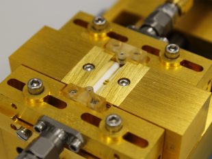
Microwave Laboratory Experts in design, packaging and testing of high reliability components Engineering Expertise The experience and technical knowledge achieved by our engineers in the last years is major lack for most space and harsh environment companies. Our engineering... Continue reading

