Assembled PCB is metallographic prepared in ALTER TECHNOLOGY Materials & Processes Laboratory, recognized as a recommended facility for such activity by ESA authority (MEMO ESA-TECMSP-MO-013165).
Sample & Method
Cross-section preparation is a very powerful way of examining the internal disposition of soldered connections, as well as analyzing potential failure mechanisms.
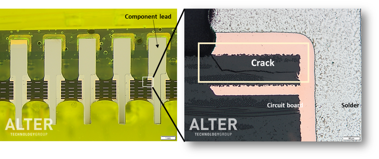
Microsection analysis is performed on an assembled through hole device as a part of a failure analysis. Cross-section through the plane of interest can provide helpfully information about solder defects, PCB inner layers and internal construction. As a part of a failure analysis, the plane of interest has to be selected taking into account PCB characteristic, observed failure and previous test results.
Remark
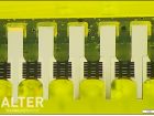
Assembling through-hole devices requires that package leads be inserted into plated through-holes in the circuit board. Once inserted, the leads are wave-soldered to secure the electrical connection.
The failure analysis reveals crack beneath pad. Cracks on the PCB are the result of mechanical stress or overload condition which may be induced by impact loads and are typically observed near the package corners.

She is responsible for the Materials & Process Laboratory of Alter Technology. Her work is focused on investigating the effects of the environment on electrical components, materials, and processes. As the head of the laboratory, she also manages the studies conducted to evaluate the quality of a bare or assembled printed circuit board in relation to ECSS standards or according to the customer’s specifications.
- MacroVoids in assembled BGA packages - 14th August 2019
- Microsection Inspection / Constructional Analysis - 23rd July 2019
- Microsection Inspection / Failure Analysis - 19th July 2019