Cross-sectioned PCB are metallographic prepared in ALTER TECHNOLOGY Materials & Processes Laboratory, recognized as a recommended facility for microsection activity by ESA authority (MEMO ESA-TECMSP-MO-013165).
Sample & Method
The separation of the interest area has to be performed in such a way as to prevent any damage by deformation or input of heat. After cleaning, the specimen is encapsulated before the grinding process takes place.
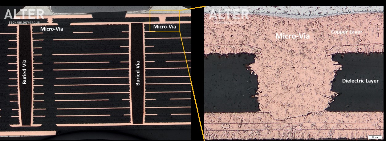
Then, rough SiC paper (500 grit) is used to rapidly achieve a surface, 1-0.5 mm away from the plane of interest. The target (the middle of the inspected vias) can be reached by using several short steps during the following processes. Considering that the time selected for each step must ensure that all deformation from the previous process is removed and the target is not reached with a rough SiC paper. Finally, the sample is polished to provide with a smooth and shiny surface to be analyzed.
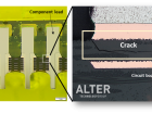
Metallographic analysis allows us to assess the reliability of the PCB.
Remark
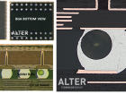
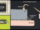
Printed Circuit Board (PCB) are metallographically inspected to ensure the quality of its multilayered structure. This test provides valuable information such as plated through-hole or via dimensions, dielectric lamination conditions, connections between the layers or inner layer copper thickness.
Specifications prepared by ECSS (ECSS-Q-ST-70-60C), NASA and IPC (IPC-6012) define acceptance and rejection criteria for PCB analysis.

She is responsible for the Materials & Process Laboratory of Alter Technology. Her work is focused on investigating the effects of the environment on electrical components, materials, and processes. As the head of the laboratory, she also manages the studies conducted to evaluate the quality of a bare or assembled printed circuit board in relation to ECSS standards or according to the customer’s specifications.
- MacroVoids in assembled BGA packages - 14th August 2019
- Microsection Inspection / Constructional Analysis - 23rd July 2019
- Microsection Inspection / Failure Analysis - 19th July 2019