Space product assurance (ECSS-Q-ST-70-38C) standard defines precisely the technical requirements and quality assurance provisions for the manufacture and verification of high-reliability electronic circuits based on surface mounted device (SMD) and mixed technology.
Additionally, the proper tools, correct materials, design and workmanship to permit discrimination between proper and improper work is defined.
However, the preparation of the samples to be inspected is a challenging task.
Microsectioning inspections
Microsectioning inspections are performed as part of the verification programme defined in the ECSS-Q-ST-70-38C standard. This test involves examining the solder connections of different electronic devices composed of different materials which properties respond in totally different ways to the sectioning method used. This implies to adapt the grinding and polishing parameters in each case.
To determine the relationship between these parameters and the quality of the inspected area, the Design of Experiments (DOE) has been a powerful tool. This methodology has allowed to identify the main variables of the sectioning process, to predict the final results and to ensure replicability.
This discussion will focus on the evaluation of different grinding processes following the results obtained from the DOE methodology.
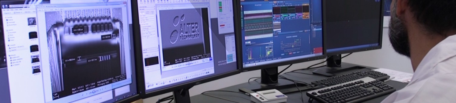
Since the sectioning process depends mainly on the hardness and ductility of the materials to grind, electronic components were grouped by their composition. For each of such families both the grinding parameters (time, pressure and rotation speed) and the abrasive materials were evaluated. In this way, the optimum process for each device has been found as it is shown in figure 1.
The use of the DOE methodology has allowed to reduce the time and the resources employed to obtain the suitability sectioning method for each electronic device. Moreover, this strategy can be implemented to identify the optimum process for each component before to submit it to a destructive test.
Techniques Materialographic Analysis Electronic Devices

Figure 1. Microsectioning area of a ceramic capacitor and a FP component using two different grinding methods. Left: Grinding process based on SiC papers. Right: Grinding process based on surfaces coated with diamond particles.
Authors: Carmen López-López, Sonia Reina, Manuel Domínguez, David Núñez Teruel.