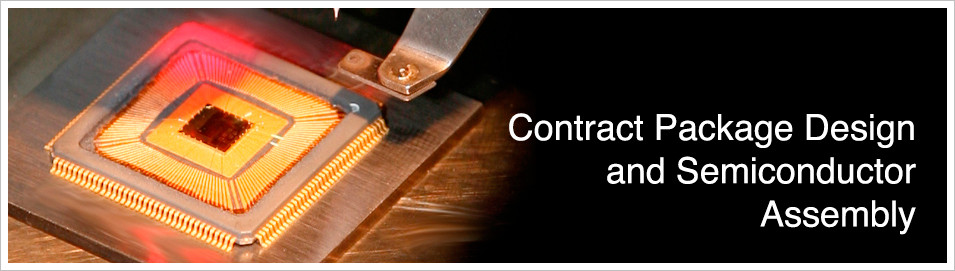
Alter Technology (formerly Optocap), offers a full range of contract precision assembly processes for semiconductor devices. Alter Technology (formerly Optocap) assembly process know-how enables reduced costs and reduced time to market for our customers.
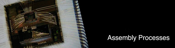
Assembly Capability
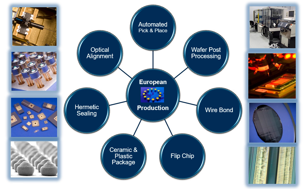


Wafer Sawing
Wafer Sawing is the process of singulating the wafer into individual die ready for subsequent assembly.
Alter Technology (formerly Optocap)has the capability for Wafer saw of substrates up to 8” diameter. When dicing of substrates of 12” diameter is required then Alter Technology (formerly Optocap) can process 12” substrates into smaller segments prior to dicing.
For many System-in-Package (SiP) applications a very thin semiconductor die is required in order to meet the demanding package form factor requirements. Alter Technology (formerly Optocap) has experience of mounting and dicing thin wafers down to 100um in thickness. Working closely with our partner companies Alter Technology (formerly Optocap)can also offer Background services and dice before Background processes to singulate die down to as little as 50um thick. In addition to handling very thin die Optocap can also dice substrates up to 1mm thick.
Alter Technology (formerly Optocap) has experience in wafer dicing a wide variety of substrates including Si, Multi-Project Wafers (MPW), GaAs, GaN, FR4, Glass, Ceramics, and Laminates. Different dicing blade thickness and materials are used depending on the substrate material and thickness.
Important parameters during wafer saw include feed speed, spindle rev, blade height, and water flow. Important parameters for the washing step include wash time, wash rpm, DI water pressure, dry time, dry rpm, temperature, and air flow rate. Alter Technology (formerly Optocap) has developed a number of optimized wafer saw and wash processes for various MEMS and Sensor devices in order to avoid damage to the sensitive membrane and optical surfaces.
Alter Technology (formerly Optocap) expertise and capability in wafer sawing will reduce risk and reduce time to market for your wafer saw requirements as well as providing a cost-effective manufacturing option.
Wire Bonding Services
Wire bonding is the main method of making interconnections between a semiconductor die and a package or substrate.
Alter Technology (formerly Optocap) works closely with our customers at the package design stage to ensure that design for manufacturing techniques are applied and wire bond design rules, where possible, are adhered to. This co-design activity is crucial in the development of high yield, fully automated and fully optimized wire bond process.
By controlling and optimizing key wire bond process and material parameters such as ultrasonic energies and wire specification a robust and reliable wire bond processes can be developed.
Alter Technology (formerly Optocap) also offers wire pull and ball shear test data to enable qualification of the wire bond process.
Alter Technology (formerly Optocap) expertise and capability in wire bonding will reduce risk and reduce time to market for your wire bonding requirements as well as providing a cost-effective manufacturing option.
Die Bonding
Die bonding is the process of attaching a die to substrate/package. Selection of the optimal die attaches material and process is based on a number of issues including thermal requirements, electrical requirements and mechanical stability.
Pick and Place
Die can be automatically picked from Gel-Pak, Waffle Pack and Wafer Film frame onto substrates and packages. For many MEMS, Sensor and Opto devices Alter Technology (formerly Optocap) utilises specially design pick-up tools to avoid damage and contact with sensitive active areas. Micron resolution dies to eject mechanisms allow for complete control of die punch-up parameters allowing thin and fragile due to being picked from wafer film frame without damage. A controlled downward force on the pick-tool is used to control the bond line thickness and ensure optimal handling of fragile semiconductor die.
Fiducial marks on die and packages enable pattern recognition software to automatically pick and place die for a repeatable high yield and high volume process.
Stud Bumping
Alter Technology (formerly Optocap) has the ability to Gold (Au) stud bump wafers and individual die making them ready for a subsequent flip chip attach process
Gold stud bumping forms Au bumps using a process very similar to Au ball wire bonding. Like wire bonding, it forms an Au ball (stud). However, the wire is terminated after the first bond so there is only a bump on the die.
Au stud bumping requires no Under Bump Metallization (UBM) or special wafer preparation, unlike the requirements for solder bumping. It also offers finer bump spacing than most solder bump technology without the added expense of a solder re-distribution layer.
Au stud bumps can be used on individual die or wafer and typically have much lower set-up costs than a solder bump approach. The ability to bump individual die makes Au stud bumping an extremely valuable tool in the prototyping phase, as well as a viable option for volume manufacturing.
For many sensitive devices such as lasers, MEMS and sensors the use of flux or adhesives is not allowed and a thermosonic or thermocompression Au-Au attach process offers a reliable flux free process to improve the device reliability.
Au stud bumps can be produced in a wide variety of diameters and shapes depending on the application. For example, Stud bumps with diameters of 40-100um can be produced with heights of 20-80um. Co-planarity of +/-2.5um can be achieved without coining process. Stacked bumps can be used to increase the stand-off distance between the die and substrate to help accommodate substrate thickness variations and minimize CTE differentials. Gold stud bumps with pointed tips can be used for subsequent epoxy dipping.
Alter Technology (formerly Optocap) expertise and capability in Gold Stud bumping will reduce risk and reduce time to market for your Gold stud bumping requirements as well as providing a cost-effective manufacturing option.
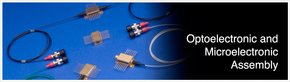
Fiber Alignment
Alter Technology (formerly Optocap) has extensive experience in aligning and attaching fibers and optical components to wide range of optoelectronic devices including DFB lasers, Quantum Cascade lasers, SLEDs, SOA’s and Receivers.
Alter Technology (formerly Optocap) offers a standard Telcordia compliant platform for packaging and fiber coupling optoelectronic devices into a 14-pin Butterfly package. This standard platform incorporates a Thermistor, Thermoelectric Cooler (TEC) and back-facet photodiode monitor. A full flux and organic free process are used to avoid any contamination that may compromise the delicate optical surfaces. A fully hermetic seal casing in an inert gas atmospheres offers an increased lifetime of the optoelectronic device. A laser welded fiber attach process is used to provide a robust and reliable attachment. This standard platform has undergone extensive environmental testing for demanding Telcordia standards.
Alter Technology (formerly Optocap) standard platform provides several key benefits;
- Avoids Design and Development NRE charges.
- Utilises Telcordia/Space compliant processes and materials.
- Enables faster time to market by utilizing off-the-shelf components and avoiding key technical pitfalls.
- Provides competitive unit prices based on automated assembly processes and utilizing economies of scales for purchasing materials.
Alter Technology (formerly Optocap) standard platform has the following features;
- Wide range of packages including 14-pin butterfly packages and TO-cans.
- PM, SM, MM, Polycrystalline, High-temperature fibers and FVA’s including lensed options.
- Laser weld or epoxy attach of the fiber assembly
- High-quality AR coating with a variety of lens designs to maximize coupling efficiency
- Solutions for a wide range of devices and wavelengths including DFB, DBR lasers, SOA’s, SLD’s VCSEL’s, Photodiodes and Quantum Cascade Lasers
- Isolators and Free-Space optics
- Thermistor, TEC and Monitor Photodiode
Encapsulation and Hermetic Sealing
Encapsulation is the process to protect die from damage after die to attach and wire bond. There are two main types of encapsulation: Glob Top and Dam and Fill.
Glob top is a process whereby a low viscosity encapsulant is dispensed on top of the die. The encapsulant flows and conforms to the shape of the die without damaging wire bonds. However, the encapsulant can flow beyond the desired area and into adjacent areas. In many applications, such as the encapsulation of MEMS devices and Concentrated Photovoltaic devices, a controlled partial encapsulation of certain selected regions, for example, wire bonds, is required but ensuring that the active surface of the device is free from the encapsulant. The tight control for partial encapsulation requires the selection of a suitable encapsulant and development of an appropriate dispense process.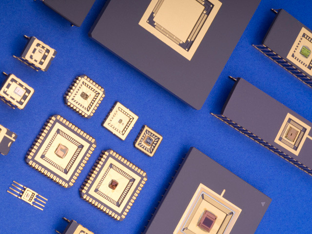
Dam and Fill encapsulant uses a dam around the die area to control the encapsulant flow within a contained area. This process can result in a much flatter encapsulation profile. It requires dispensing of two or more encapsulant materials in the same dispense program during an automated process.
Variations of the above processes can be used to fully encapsulate Open-Cavity Plastic Packages. Using a subsequent flattening technique on the encapsulant the package can meet the original JEDEC form-factor standards and provide test socket compatibility.
Alter Technology (formerly Optocap) also has experience with a range of optically clear encapsulant and silicones for protecting devices such as LEDs and Photovoltaic’s. Optocap also supports customers with the design and procurement of frames suitable for containing the encapsulant material.
Hermetic Sealing
Alter Technology (formerly Optocap) provides hermetic sealing of various metal package configurations including TO-can style package and Butterfly packages.
Parallel resistance welding is used for rectangular or square packages. Projection welding is used for TO-can devices.
Prior to sealing parts, they are put through a Vacuum bake-out process to remove moisture and other residues from the component surface. Devices can be hermetically sealed in a wide variety of inert gas atmospheres including N2, Ar, O2, depending on the customers’ exact requirements.
Fine and Gross leak tests are carried out to MIL-STD-883. Alter Technology (formerly Optocap) has achieved leak rates of <5E-9 for a fiber-coupled butterfly package. This offers the potential of reducing the length of lifetime tests in certain applications.
Alter Technology (formerly Optocap) expertise and capability in Encapsulation and Hermetic Sealing will reduce risk and reduce time to market as well as providing a cost-effective manufacturing option.
- Quantum Key Distribution - 7th November 2022
- Conducted Immunity - 20th May 2019
- Electrical transients Test - 2nd May 2019