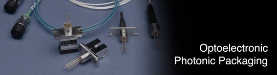
Optoelectronic Photonic Packaging
A key function of an optoelectronic device is to manipulate light. As a result, the packaging and assembly processes for many optoelectronic components can be significantly more complex than traditional microelectronic devices.
Optoelectronic or Photonics packaging requires extremely accurate placement of components to ensure appropriate suitable alignment and coupling of light into and out of devices. In many cases the generation or detection of light results in significant heat being generated, which if not suitably dissipated through appropriate joining technology and material selection, can adversely affect the device operation. Additionally, assembly processes can be complicated by the requirement that fluxes and other organic materials can’t be used as they can degrade the performance of facets in optical devices.
Alter Technology (formerly Optocap), has experience in the assembly and packaging of a wide range of Optoelectronic devices including;
- High power laser diodes
- PV Cells
- Optical Interconnects
- DFB’s, SOA’s
- Mach-Zender Interferometers
- Modulators
- Photodetectors
- TOSA/ROSA’s
Alter Technology UK, expertise and capability in Optoelectronic Photonic Packaging will reduce risk and reduce time to market for your Optoelectronic packaging requirements as well as providing a cost-effective manufacturing option.
Laser Diode Packaging
Alter Technology UK, offers customers support in both prototype/process development for laser diode packaging as well as volume manufacturing capability.
By prototyping on the volume manufacturing tool-set Alter Technology UK can offer a risk-free transition to manufacturing with a fully optimised and high yield process.
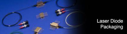
A summary of Alter Technology UK laser diode packaging expertise can be found below;
- Process Highlights
- Placement accuracies from +/- 1µm to +/-20µm
- Fully automated or manual placement
- Adjustable bond force
- 3-axis placement control
- Void free Eutectic die attach
- Control of flatness “smile”
- Epi-side down or up assembly
- Vacuum reflow processes
- Materials
- GaAs or InP
- Size
- Laser bars in excess of 10mm
- Laser single emitters to 5mm
- Package Type
- C-mount (standard sizes of 4mm to 5mm, sharp edge for accurate placement)
- CS-mount
- TO-can
- Stacks
- Eutectic solder processes including AuSn, SnAg, InAg, SnPb, BiSn (preforms, pre-deposited substrates to control solder overspill
- CuW/Cu/AlN/CuW/CVD Diamond sub-mounts and heat-sinks
Alter Technology UK expertise and capability in Laser Diode Packaging will reduce risk and reduce time to market for your laser diode packaging requirements as well as providing a cost-effective manufacturing option.
LED packaging
Alter Technology UK has extensive experience in the packaging high brightness LEDS (HB-LEDS).
Alter Technology UK, offers customers support in both prototype/process development for LED packaging as well as volume manufacturing capability. By prototyping on the volume manufacturing tool-set Optocap can offer a risk-free transition to manufacturing with a fully optimised and high yield process.
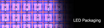
A case-study for a LED packaging application can be found below;
- Multiple LED attached to a single substrate and individually interconnected.
- LED die presented on Wafer Film Frame. Die ejected from film frame use precisely controlled die ejector needle to avoid damage to LED die.
- Epoxy stamped (daubed) onto a substrate with a diameter of 200um to provide required die-attach coverage and thermal dissipation.
- LED die pick and placed onto a substrate in a fully automated process.
- 25um Au wire bonding to individually wire bond each LED die.
- Frame attached round substrate and encapsulated with Silicone to provide suitable surface quality for transmission of LED light.
- Optics attached to the surface to provide shaping of light.
- Populated module attached to heat-sink with solder attaches process.
Alter Technology UK expertise and capability in LED Packaging will reduce risk and reduce time to market for your LED packaging requirements as well as providing a cost-effective manufacturing option.
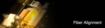
Fiber Alignment
Alter Technology UK, offers a standard Telcordia compliant platform for packaging and fibre coupling optoelectronic devices into 14-pin Butterfly package. This standard platform incorporates a Thermistor, Thermoelectric Cooler (TEC) and back-facet photodiode monitor. A full flux and organic free process are used to avoid any contamination that may compromise the delicate optical surfaces. A fully hermetic seal casing in an inert gas atmospheres offers an increased lifetime of the optoelectronic device. A laser-welded fibre attach process is used to provide a robust and reliable attachment. This standard platform has undergone extensive environmental testing for demanding Telcordia standards.
Alter Technology UK, the standard platform provides several key benefits;
- Avoids Design and Development NRE charges.
- Utilises Telcordia/Space compliant processes and materials.
- Enables faster time to market by utilising off-the-shelf components and avoiding key technical pitfalls.
- Provides competitive unit prices based on automated assembly processes and utilising economies of scales for purchasing materials.
Alter Technology UK, the standard platform has the following features;
- Wide range of packages including 14-pin butterfly packages and TO-cans.
- PM, SM, MM, Polycrystalline, High-temperature fibres and FVA’s including lensed options.
- Laser weld or epoxy attach of fiber assembly
- High-quality AR coating with a variety of lens designs to maximise coupling efficiency
- Solutions for a wide range of devices and wavelengths including DFB, DBR lasers, SOA’s, SLD’s VCSEL’s, Photodiodes and Quantum Cascade lasers
- Isolators and Free-Space optics
- Thermistor, TEC and Monitor Photodiode
Contact us for more information
- Quantum Key Distribution - 7th November 2022
- Conducted Immunity - 20th May 2019
- Electrical transients Test - 2nd May 2019