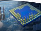
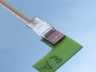
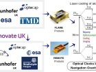
Laser Diode Packaging
Alter Technology (formerly Optocap), offers customers support in both prototype/process development for laser diode packaging as well as volume manufacturing capability.
 By prototyping on the volume manufacturing tool-set Alter Technology UK, can offer a risk-free transition to manufacturing with a fully optimised and high yield process.
A summary of Alter Technology UK, laser diode packaging expertise can be found below;
- Process Highlights
- Placement accuracies from +/- 1µm to +/-20µm
- Fully automated or manual placement
- Adjustable bond force
- 3-axis placement control
- Void free Eutectic die attach
- Control of flatness “smile”
- Epi-side down or up assembly
- Vacuum reflow processes
- Materials
- GaAs or InP
- Size
- Laser bars in excess of 10mm
- Laser single emitters to 5mm
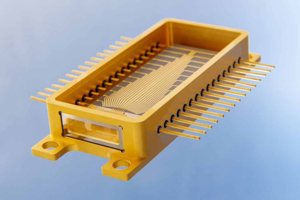
- Package Type
- C-mount (standard sizes of 4mm to 5mm, sharp edge for accurate placement)
- CS-mount
- TO-can
- Stacks
- Eutectic solder processes including AuSn, SnAg, InAg, SnPb, BiSn (preforms, pre-deposited substrates to control solder overspill
- CuW/Cu/AlN/CuW/CVD Diamond sub-mounts and heat-sinks
Alter Technology UK, expertise and capability in Laser Diode Packaging will reduce risk and reduce time to market for your laser diode packaging requirements as well as providing a cost-effective manufacturing option.
Contact us for more information
Latest posts by Media ATN (see all)
- Quantum Key Distribution - 7th November 2022
- Conducted Immunity - 20th May 2019
- Electrical transients Test - 2nd May 2019