Alter Technology (formerly Optocap), offers customers support in both prototype/process development for RF Module packaging as well as volume manufacturing capability.
By prototyping on the volume manufacturing tool-set Alter Technology UK can offer a risk-free transition to manufacturing with a fully optimised and high yield process.
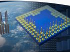
 RF Module Packaging
As RF modules run at very high frequencies the effects of capacitance and stray inductance become even more important. The RF module must be designed and assembled with an understanding of these effects.
A summary of Optocap’s RF Module packaging expertise can be found below;
- Process Highlights
-
- Controlled wire-bonding on automated equipment for optimal wire bond loop profile
- Wire bond length control less than 75um
- Gold ball
- Wedge-Wedge
- Ribbon bonding (25umx50um, 25umx75um)
- Non-contact handling process for MMIC die
- Accurate placement of die to transmission lines
-
- Materials
- Substrates: Duroid, FR4, Ceramics
- Conductive or Eutectic Die attach
- Products: RF transmitter/receiver modules/Optical RF Modules
Alter Technology UK expertise and capability in RF Module Packaging will reduce risk and reduce time to market for your laser RF module packaging requirements as well as providing a cost-effective manufacturing option.
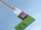
Photonic Packaging
A key function of an optoelectronic device is to manipulate light. As a result, the packaging and assembly processes for many optoelectronic components can be significantly more complex than traditional microelectronic devices.
Optoelectronic or Photonics packaging requires extremely accurate placement of components to ensure appropriate suitable alignment and coupling of light into and out of devices. In many cases the generation or detection of light results in significant heat being generated, which if not suitably dissipated through appropriate joining technology and material selection, can adversely affect the device operation. Additionally, assembly processes can be complicated by the requirement that fluxes and other organic materials can’t be used as they can degrade the performance of facets in optical devices.
Alter Technology UK has experience in the assembly and packaging of a wide range of Optoelectronic devices including;
- High power laser diodes
- PV Cells
- Optical Interconnects
- DFB’s, SOA’s
- Mach-Zender Interferometers
- Modulators
- Photodetectors
- TOSA/ROSA’s
Alter Technology UK expertise and capability in Optoelectronic Photonic Packaging will reduce risk and reduce time to market for your Optoelectronic packaging requirements as well as providing a cost-effective manufacturing option.
Contact us for more information
- Quantum Key Distribution - 7th November 2022
- Conducted Immunity - 20th May 2019
- Electrical transients Test - 2nd May 2019