ALTER TECHNOLOGY TÜV NORD | Web Project Office Alter Technology
MENUMENU
  • SERVICES
    • Engineering & testing of Hi Rel Components
      • ACCEPTANCE TESTS
      • COTS Commercial Off-The-Shelf | EEE Parts
      • COUNTERFEIT DETECTION, AUTHENTICITY TESTS
      • EVALUATION / QUALIFICATION
      • ELECTRICAL CHARACTERIZATION
      • FAILURE ANALYSIS
      • MATERIAL & PROCESSES Laboratory
      • MICROSECTIONING
      • MICROWAVE TESTING
      • PARTS ENGINEERING & LOGISTIC
      • PROCUREMENT EEE Parts
      • RADIATION TESTING
      • RELIFING
      • Scanning Acoustic Microscopy C-SAM
      • SCREENING
      • TIN WHISKERS GROWTH
      • VIBRATION TESTING
    • Packaging & Assembly
      • APPLICATIONS
      • ASSEMBLY PROCESSES
      • DESIGN
    • Certification & Equipment Testing
      • CE MARKING
      • CERTIFICATION OF INTRUSION AND ALARMS PRODUCT
      • INDUSTRY & SECURITY
      • LABORATORY TESTS
      • DIGITAL SERVICES
    • DRONES (Remotely Piloted Aircraft Systems)
      • REGULATION & NORMATIVE
      • SERVICES to DRONE INDUSTRY
    • Innovation
      • Quantum Key Distribution
      • Photonic Technologies in Space Applications
  • PROJECTS
  • PRODUCTS
    • doEEEt - Tool of Hi-Rel Parts for Use in Space
    • SMALL SATELLITES - NEW SPACE
    • SILICON CARBIDE POWER DIODES
    • FLAME – FREQUENCY Stabilised Laser
    • REMOTE - EXTERNAL CAVITY DIODE LASER
    • 19" FRONT PANEL TL-FP-3421 - Galileo System
  • PUBLICATIONS
  • CONTACT
    • Alter Technology Spain (Seville)
    • Alter Technology Spain (Madrid)
    • Alter Technology France
    • Alter Technology UK
  • User Area

Tag - microscopy

MacroVoids in assembled BGA packages
  • Microsectioning
  • Short Technical Notes

MacroVoids in assembled BGA packages

by MC Lopez

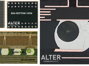
BGA device assembled to a PCB has been submitted to the ECSS verification programme following the guideline defined in the ECSS standard ECSS-Q-ST-70-38C.

Constructional Analysis
  • Microsectioning
  • Short Technical Notes

Microsection Inspection / Constructional Analysis

by MC Lopez

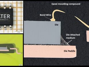
Cross-section analysis is a very useful way of determining the construction and material composition of electronic devices. The FP device is potted in epoxy resin. After curing, the sample is sequentially grinded up to reach the plane of interest. Then, the specimen is subjected...

CLSMb
  • Material Processes
  • Microwave & RF testing

Noncontact 3D Characterization Using Confocal Laser Scanning Microscopy (CLSM)

by Fernando Teberio

At Alter Technology, we can perform 3D characterization using Confocal Laser Scanning Microscopy and the world’s most integrated and flexible test equipment for nondestructive 3D dimensional characterization, helping designers to get in-depth information about their prototypes.

  • Material Processes

Fluorescence Microscopy + dye penetrant test | EEE Parts

by Francisco Javier Aparicio Rebollo

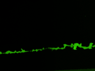
This technique combines to two inspection methods (microscopy and fluorescent dye penetrant inspection) commonly used for the detection of surface anomalies such as cracks, porosity, laps, delaminations, and other discontinuities. This joint approach is intended to highlight and...

  • Evaluation / Qualification
  • Material Processes

Raman Thermometry | Hi Rel Electronics Parts

by Francisco Javier Aparicio Rebollo

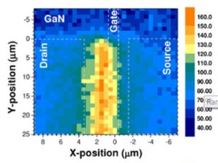
Raman thermometry is a thermal characterization technique which makes use of Raman scattering phenomena to determine the local temperature in microelectronics systems. Non-contact character. High spatial resolution (sub-micron scale). In-depth analysis within IR-transparent...

  • Evaluation / Qualification
  • Material Processes

IR Thermal Microscopy | Hi Rel Parts

by Francisco Javier Aparicio Rebollo

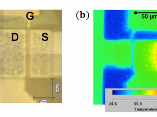
IR thermal microscopy (or infrared radiation thermometry) analyses the spatial distribution of the emitted infrared radiation either over the device surface or eventually inside the inspected device. This technique enables us to obtain 2D temperature maps, which are used to...

scanning electron microscope SEM FIB
  • Acceptance tests
  • Evaluation / Qualification
  • Material Processes

Scanning Electron Microscope SEM – FIB Inspections Focused Ion Beam | Hi Rel Parts

by Francisco Javier Aparicio Rebollo

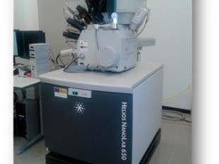
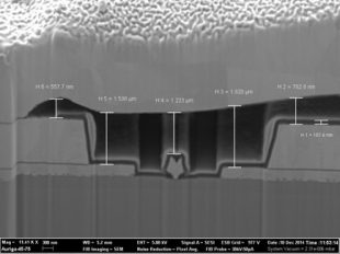
This type of inspection is performed using an electron microscope which produces images of a sample by scanning it with a focused electron beam. Interaction between the electrons and atoms in the sample generates signals that contain information about the sample’s surface...

helios nanolab 650
  • Acceptance tests
  • Evaluation / Qualification
  • Failure analysis
  • Material Processes

SEM EDS, Internal Material Analysis | EEE Parts

by Francisco Javier Aparicio Rebollo

This analytic technique may provide both qualitative and quantitative information of the composition of a surface, i.e. identification of the elements and the element weights, respectively. The technique relies on the detection and spectroscopy of secondary radiation (X-Ray)...

Microsectioning
  • Acceptance tests
  • Evaluation / Qualification
  • Failure analysis
  • Material Processes

Focused Ion Beam (FIB) Micro-Sectioning | HI Rel Parts

by Francisco Javier Aparicio Rebollo

Focused ion beam, also known as ion milling, is a technique used particularly in the semiconductor industry and materials science for site-specific analysis, deposition and ablation of materials. Since it is destructive to the part, FIB technology is used for micro-sectioning in...

Follow Us

  • facebook
  • twitter
  • linkedin
  • googleplus
  • youtube
  • vimeo
Copyright © 2019. ALTER TECHNOLOGY TÜV NORD S.A.U
  • Contact
  • Privacy Policy and Legal Notice
  • Cookies
  • English
  • Español