SEM – EDS
This analytic technique may provide both qualitative and quantitative information of the composition of a surface, i.e. identification of the elements and the element weights, respectively. The technique relies on the detection and spectroscopy of secondary radiation (X-Ray) emitted when a high intensity incident beam of electrons impinges upon the materials placed in its path. The SEM – EDS Internal Material Analysis (also known as EDX or EDAX) can be performed in accordance with MIL-STD-883, MIL-STD-750, MIL-STD-1580 and ESCC 25500 requirements.
Our SEM has the capability of delivering at a minimum a 20 kV electron beam onto the surface of the material being analyzed for the purpose of detecting the presence of prohibited materials. The EDS system is capable of quantitatively identifying the weight percentage of each element of the material being analyzed and has the ability to generate EDS spectra and quantitative data in a complete report format.
The test samples should be prepared in such a manner as to optimize the results of the analysis. Coatings to provide a ground path should be carefully chosen. Moreover, materials used in coatings should be chosen such that they do not interfere with achieving the best analysis of the materials in the sample. Whenever possible, a cross-sectioned sample having a flat area of analysis is recommended.
A first surface inspection with the SEM – EDS technique will aim at microscopically characterizing the sample so as to establish a good understanding of its microcrystalline structure and morphology. Additionally, the SEM – EDS may also help discriminate cases in which the limits of the quantitative resolution of the XRF system may lead to non-conclusive results of that test.
Scanning Electronic Microscopes
HELIOS NANOLAB 650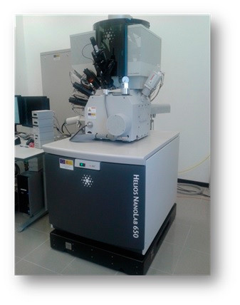
- Top-model Dual Microscope from FEI. The SEM column (Elstar XHR immersion lens FESEM column) has a resolution of 0.8nm at 15 kV and 0.9 nm at 1 kV
- Designed to access a new world of extreme high-resolution (XHR) 2D and 3D characterization, nanoprototyping, and higher quality sample preparation
Since 2007 Dr Aparicio has developed a productive research career within the field of Materials Science including post-doctoral stays at the University of Trento, the University of Mons, and the Spanish National Research Council (CSIC). His researches have been published in more than 30 articles in reputed international research journals and conferences (> 70) including more than 10 invited talks and lectures.
Within the frame of the programme “Torres Quevedo” for the Knowledge Transfer and the incorporation of research talent into the industry, in 2019 he joined Alter Technology as Senior Materials Science Test Engineer. In 2019 he was appointed to lead the Scanning Acoustic Microscopy Service. Within this framework, he currently collaborates in different ESA projects (JUICE and PLATO).”
- Scanning Acoustic Microscopy on Ceramic Capacitors - 18th May 2020
- Non-destructive detection of micrometric internal features within EEE microelectronic systems. - 3rd September 2019
- Acoustic Inspection of Hybrid Systems on Laminated Substrates - 3rd September 2019