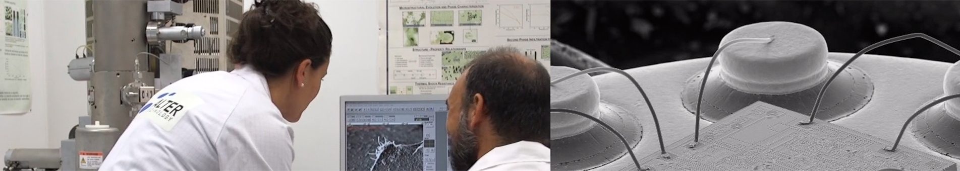
Scanning Electron Microscope SEM – FIB Inspections Focused Ion Beam
SEM available high magnification tool to analyse the design, construction or handling defects. It can be used to check the interconnect metallization on integrated circuit: metal step coverage, etc., or for performing an in-depth technology study: reverse engineering, die cross sectioning, failure analysis, etc.
This type of inspection is performed using an electron microscope which produces images of a sample by scanning it with a focused electron beam. Interaction between the electrons and atoms in the sample generates signals that contain information about the sample’s surface topography and elemental composition.
The three signals that provide the greatest amount of data are the secondary electrons, backscattered electrons, and X-rays. Secondary electrons are emitted from the top surface atoms, producing a readily interpretable, high-resolution image of the surface topographic features with magnification up to 100,000x and spatial resolution better than 50Å. Backscattered electrons are primary beam electrons reflected from atoms in the solid, the image produced showing the chemical phase distribution in the sample.
The X-ray emission caused by the interaction of the primary beam with atoms in the sample reveals the energy spectra providing qualitative and quantitative elemental composition as well as showing the elemental distribution in a sample surface (EDS).
This test technique is useful for analyzing the design or construction or for defect handling. It also can be used to check the interconnect metallization on integrated circuits, metal step coverage, etc., or for performing an in-depth technology study: reverse engineering, die cross-sectioning, failure analysis, etc.
Additionally, the SEM equipment can be complemented with such devices as a XRF/EDS system (for qualitative and quantitative elemental analysis) or an FIB setup (for micro-sectioning).
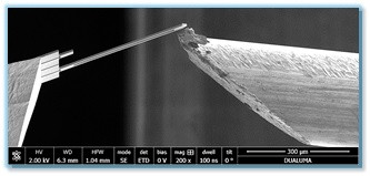
Alter Technology performs FIB using a FEI top-model Dual microscope. The SEM column (Elstar XHR immersion lens FESEM column) has a resolution of 0.8nm at 15kV and 0.9nm at 1kV, and is designed to access an extremely high-resolution (XHR) 2D and 3D characterization, nanoprototyping, and higher quality sample preparation.
Precise cross-section analysis
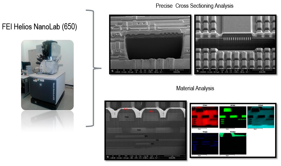
Material analysis
Depending on the parts and the area to be inspected, SEM examinations are performed in accordance with different standards such as MIL-STD-750 method 2077 or MIL-STD-883 method 2018, among others. As an example, method 2018 of MIL-STD-883 provides a means of judging the quality and acceptability of device interconnect metallization on non-planar oxide integrated circuit wafers or dice while performing SEM on glassivated devices.
 [simple-author-box]

Since 2007 Dr Aparicio has developed a productive research career within the field of Materials Science including post-doctoral stays at the University of Trento, the University of Mons, and the Spanish National Research Council (CSIC). His researches have been published in more than 30 articles in reputed international research journals and conferences (> 70) including more than 10 invited talks and lectures.
Within the frame of the programme “Torres Quevedo” for the Knowledge Transfer and the incorporation of research talent into the industry, in 2019 he joined Alter Technology as Senior Materials Science Test Engineer. In 2019 he was appointed to lead the Scanning Acoustic Microscopy Service. Within this framework, he currently collaborates in different ESA projects (JUICE and PLATO).”
- Scanning Acoustic Microscopy on Ceramic Capacitors - 18th May 2020
- Non-destructive detection of micrometric internal features within EEE microelectronic systems. - 3rd September 2019
- Acoustic Inspection of Hybrid Systems on Laminated Substrates - 3rd September 2019