Assessing Radiation Hardness of SIC MOS Structures
Centro Nacional de Microelectrónica (CNM) Instituto de Microelectrónica de Barcelona (IMB), Barcelona (Spain)
Motivation and Study Strategy
This study aims to support the development of discrete European radiation hardened SiC power MOSFET for use in space applications by means of studying the gate oxide in terms of SEE and TID as one of the key parameters in the future development of these devices. The resistance of the P/N junctions present in these devices was also studied as well taking into account the problems seen in Schottky junctions under heavy ions radiation combined with high voltage.
The following approach to better understand SiC Power MOSFET sensitivity was followed:
- Gate Oxide oxidation process and gate geometry study: 3 oxidation processes + 5 gate geometries tested under gamma and heavy ions
- Heavy Ions test of 600V HV L-DMOS with experimental boron-doped gate oxide that could improve radiation hardness
- Heavy ions onto 1200V PIN diodes fully representative of the built-in ones present in power MOSFETs
Gate Oxidation Processes & Geometries
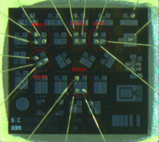
DUTs description: SiC Lateral MOS
- Ox1: Thermally grown gate thin SiO2 oxide in N2O ambient + TEOS deposition 400 Å
- Ox2: Thermally grown gate SiO2 oxide + Boron doped 1 + TEOS 400 Å
- Ox3: Thermally grown gate thin SiO2 oxide in N2O ambient + TEOS deposition 400 Å with oxidation process optimization
Results:
- No failures under heavy ions beams up to LET=62.5MeV /mg/cm2
- Total recovery after annealing for gamma (300Krad)
- Small differences among oxide types and no difference among gate geometries
Gate Oxidation Results
| wdt_ID | DUT | Gate Width (μm) | Gate Length (μm) | Channel Rotation Vs flat (11-20) (°) |
|---|---|---|---|---|
| 1 | MOS1 | 2 | 150 | 0 |
| 2 | MOS2 | 4 | 150 | 0 |
| 3 | MOS3 | 24 | 150 | 0 |
| 4 | MOS4 | 4 | 300 | 0 |
| 5 | MOS5 | 24 | 150 | 30 |
| DUT | Gate Width (μm) | Gate Length (μm) | Channel Rotation Vs flat (11-20) (°) |
HV L-DMOS Under Heavy Ions 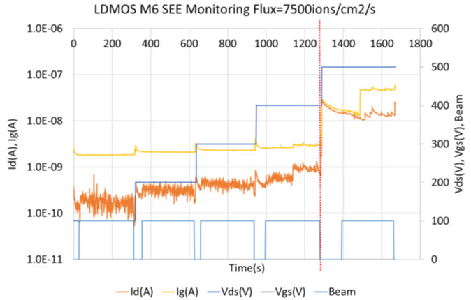
Catastrophic damage of the devices for bias values as low as VDS=200V for LET values of 32.4 and VDS=400V for 20.4 MeV/cm2/mg(Si). The damage occurs during radiation while biasing or during intermediate PIGS after a step.
Results:
| wdt_ID | LET | VGS (V) | VDS (V) | Damage |
|---|---|---|---|---|
| 1 | 10.0 | 0, 2.5, -5 | 0 | no |
| 2 | 20.4 | 0, 2.5, -5 | 0 | no |
| 3 | 32.4 | 0, 2.5, -5 | 0 | no |
| 4 | 10.0 | 0 | up to 500 | no |
| 5 | 20.4 | 0 | up to 500 | PIGS after 400V run |
| 6 | 32.4 | 0 | up to 500 | PIGS after 200V run |
| 7 | 62.5 | 0 | up to 500 | 200V run |
| 8 | 20.4 | -5 | up to 500 | 400V run |
| 9 | ||||
| LET | VGS (V) | VDS (V) | Damage |

PIN Diodes Under Heavy Ions 
Built-in diodes tested separately revealed the sensitivity of this area of the power MOSFET to heavy ions while HV is applied. Damage of the PIN occurs for reverse voltages slightly higher than for Schottky of previous studies.
Results:
| wdt_ID | DUT | LET | Vrev Step (V) | Failure at |
|---|---|---|---|---|
| 1 | PiN1 | 10.0 | 100 | abrupt failure @500V |
| 2 | PiN2 | 20.4 | 100 | abrupt failure @500V |
| 3 | PiN3 | 32.4 | 100 | degradation @400V |
| 4 | PiN4 | 62.5 | 100 | degradation @400V |
| 5 | PiN7 | 20.4 | 25 | degradation @400V |
| 6 | PiN8 | 20.4 | 20 | degradation @420V |
| 7 | PiN9 | 32.4 | 25 | degradation @400V |
| 8 | PiN11 | 32.4 | 20 | degradation @400V |
| DUT | LET | Vrev Step (V) | Failure at |
Conclusion
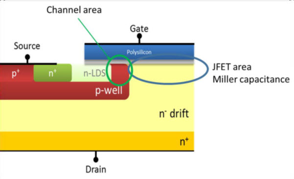
– SEE testing of the lateral MOS revealed no sensitivity of the devices to heavy ions. A possible explanation for this could be that damage in
vertical DMOS is mainly located in the JFET area between p-wells which is submitted to higher electric fields. No important differences could be detected comparing oxidation processes and gate geometries. However, slightly better behaviour under gamma radiation was observed for the devices with boron doped devices.
– SEE testing of the L-DMOS: In vertical power devices, the weak area is the JFET zone located below the gate between the p-wells. In the LDMOS, there is no JFET area as the top cell is not symmetrical. In these structures, the high peak of electric field is usually at the end of the gate metallization where probably was located the breakdown point during our campaign. While in vertical power MOSFETs, the breakdown is taking place in the bulk, either in the P-well junction or in the termination junction.
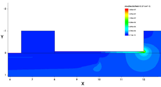 Modelling of the electric field distribution in the LDMOS at 500V clearly shows the peak electric field located at the end of the gate metal. A clear improvement of this device could be then to increase the oxide below the metal in the gate end. For the L-DMOS under
 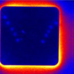 test, the damage is located in a different area than in the vertical DMOS. This explains degradation happening during irradiation steps, while in a vertical structure, the damage is usually revealed during PIGS.
– SEE testing of 1200V PIN diodes revealed sensitivity to ions but better behavior than 1200 Schottky diodes. The dependence of the damage with LET is also lower for PIN diodes. Thermographic analysis of damaged devices shows different failure modes for different devices, observing both uniform damage in the junction 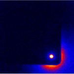 area and local hot spots probably located in already defective spots of the crystal depending on the sample analyzed.
Acknowledgments
Project funded by European Space Agency, AO/1-8081/14/NL/KML “Prototyping and Characterization of Radiation Hardened SiC MOS Structures”
- Quantum Key Distribution - 7th November 2022
- Conducted Immunity - 20th May 2019
- Electrical transients Test - 2nd May 2019