The continuous development and rise of integrated electronic devices is continually decreasing the typical distances and dimensions of their elemental components. Miniaturization is accompanied by problems due to excessive internal heating, to the extent that it is responsible for critical failures. For instance, inappropriate dissipation and heat generation can lead to reduced electron mobility. In integrated circuits and other microelectronic systems the dimension of the generated hot-spots can be limited at the micrometric or submicrometric range. Hence, such thermal singularities required for of advanced diagnostic techniques capable of detecting temperature gradients at the microscopic scale.
Why IR Thermal Microscopy
IR thermal microscopy (or infrared radiation thermometry) analyses the spatial distribution of the emitted infrared radiation either over the device surface or eventually inside the inspected device. This technique enables us to obtain 2D temperature maps, which are used to detect temperature gradients and hot spots. Along with Raman thermometry and thermoreflectance thermal imaging, it constitutes one of the main non-contact techniques (optical methods) for thermal analysis. IR thermometry presents several other benefits:
- Non-contact.
- Temperature resolution ranging from 10 – 50 °C depending on the used equipment.
- Transient and static temperature maps for hot spots identification.
- Possibility of inside analyses.
- High spatial resolution .
- Large-area overview (of the order of ).
- Time resolution .
Amongst them it is worth remaking the capability of performing bulk analyses of silicon embedded objects. This is so thanks to the transparency of silicon at near infrared wavelengths.
Complementary to Raman thermometry
IR radiation microscopy is an advantageous technique to map the temperature over large areas and for the fast location of hot-spots, which is the main goal of this method when applied to ICs and microelectronic components. Although the method provides lower temperature and spatial resolution in comparison to Raman thermometry, it has shorter acquisition time to register full-field temperature maps. All this makes them complementary techniques when implemented in the same microscope.
Practical case
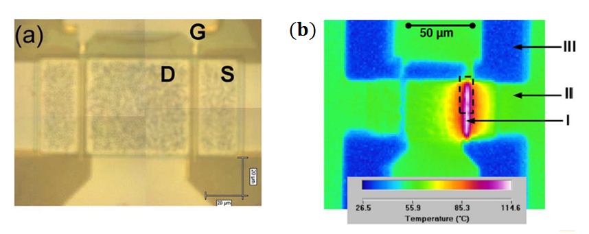
 The figure above compares an optical image (a) and an infrared image (b) of the same transistor from the underside view. This transistor is an AlGaN/GaN HFET structure with two 2×50 fingers. In the thermal image on the left we can distinguish three different areas: (I) hot-spot, (II) area covered by metal contacts and (III) area without metal contacts. The transistor in the IR system image has a source-drain bias of 40 V and 25 mA. The thermal image clearly shows that one of the fingers is operative (red area at ≈ 114 ºC) and also shows the heating of the metal-coated areas (green zones ≈ 60 ºC) in constant with the non-coated areas which are thermally isolated form the hot spot (blue zones at room temperature).
How it works
IR thermal microscopy operation principle is based on the detection of the electromagnetic radiation emitted by any body as result of their thermal characteristics. The ideal case to illustrate this phenomenon is the black-body whose total thermal radiation has the following dependence with temperature:
j = ε · σ · T4
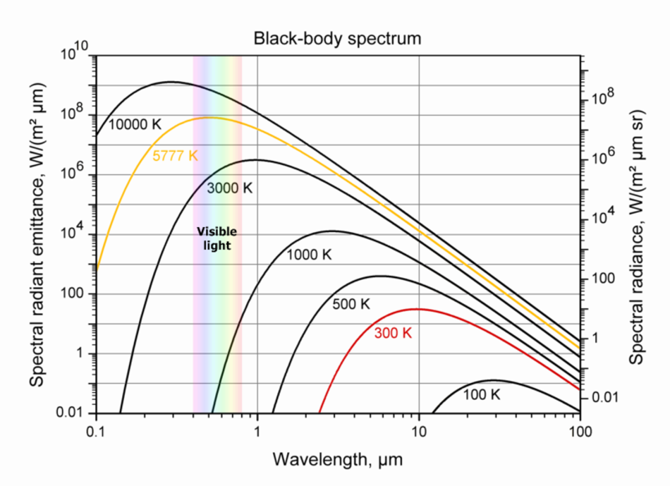
Where stands for the total thermal radiation, is the body emissivity, stands for the temperature and is the Stefan-Boltzmann constant, being the total thermal radiation equivalent to the area under each curve on the figure below.
Radiation density depends on temperature and wavelength, as it can be seen in the following figure. Therefore, at the operational temperature for electronic devices and typical hot spots temperatures (between 300 and 600 K), the electromagnetic radiation emitted by these devices fall within the near infrared range. Hence specific IR detectors and specific optical systems are required for these applications.
- Scanning Acoustic Microscopy on Ceramic Capacitors - 18th May 2020
- Non-destructive detection of micrometric internal features within EEE microelectronic systems. - 3rd September 2019
- Acoustic Inspection of Hybrid Systems on Laminated Substrates - 3rd September 2019


