Summary
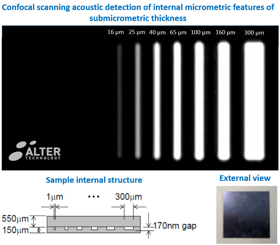
Micrometric-wide internal features of sub-micrometric thickness can be easily detected in our recently upgraded instrument. The high lateral resolution is within the current state of the start in the non-destructive inspection of deeply embedded objects.
Introduction
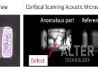
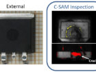
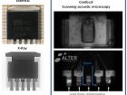
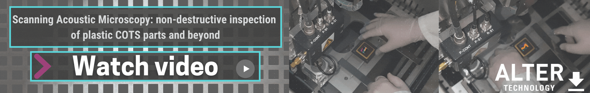
Scanning Acoustic Microscopy has proved to be a very powerful tool for the non-destructive detection of nanometre-thick defects (voids, cracks, and delamination) in plastic encapsulated microelectronic systems (diodes and semiconductors, integrated circuits and rid systems and others). However, the technique may present limitations in terms of lateral resolution when dealing with the detection of small area features. In this regards, lateral-sensitivity tests analyzing the detection limit of narrow features are taken of an indication to assess whether the instrument is reliable and accurate enough for a given application (e.g. the inspection of submillimetre packages with embedded micrometric parts).
Our Capabilities
Our recently upgraded capabilities allow us to detect micrometric features down to 16-25 µm as illustrated in the image. This confocal scanning acoustic microscopy inspection (CSAM) was conducted on a Si bonded wafers with artificial slots fabricated of submicrometric thickness (170 nm). The detected features are below a 0.5-mm-thick layer of silicon.
The high lateral resolution is within the current state of the start in the inspection of embedded objects. Smaller defects can be detector by increasing the transducer frequency, up to the GHz range, but in that cases the inspection depth is circumscribed to the subsurface regions, which precludes the inspection of critical parts in deep locations.
Contact us
Since 2007 Dr Aparicio has developed a productive research career within the field of Materials Science including post-doctoral stays at the University of Trento, the University of Mons, and the Spanish National Research Council (CSIC). His researches have been published in more than 30 articles in reputed international research journals and conferences (> 70) including more than 10 invited talks and lectures.
Within the frame of the programme “Torres Quevedo” for the Knowledge Transfer and the incorporation of research talent into the industry, in 2019 he joined Alter Technology as Senior Materials Science Test Engineer. In 2019 he was appointed to lead the Scanning Acoustic Microscopy Service. Within this framework, he currently collaborates in different ESA projects (JUICE and PLATO).”
- Scanning Acoustic Microscopy on Ceramic Capacitors - 18th May 2020
- Non-destructive detection of micrometric internal features within EEE microelectronic systems. - 3rd September 2019
- Acoustic Inspection of Hybrid Systems on Laminated Substrates - 3rd September 2019