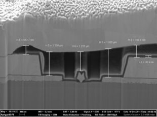
Focused ion beam, also known as ion milling, is a technique used particularly in the semiconductor industry and materials science for site-specific analysis, deposition and ablation of materials. Since it is destructive to the part, FIB technology is used for micro-sectioning in...
The cross-sectioning process provides access to the device internal structure, its materials and design. Such components as diodes and capacitors and silicon dice are often subjected to cross-sectioning to detect the defects which could not be found using other testing...

Decapsulation of packaged devices exposes the internal elements of the device under test. Opening devices by this method allows the inspection of the die, interconnects and other features typically examined during failure analysis (FA), constructional analysis (CA) and...
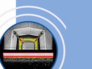
Scanning Acoustic Microscopy (SAM) is an inspection that uses focused sound to investigate, measure, or obtain an internal image of an object. It is commonly used in failure analysis and non-destructive evaluation. The semiconductor industry has found the SAM, particularly the C...

Lead integrity test is performed to determine the integrity of the device leads (terminals), welds and seals. During the execution of this test, the DUT is subjected to various stresses including tension, bending fatigue and torque. The stresses to be applied depend on the DUT...

is performed to evaluate the reliability of non-hermetic packaged solid-state devices that are likely to encounter humid environments during normal (ambient) operation. Also known as Pressure Cooker Test (PCT) or Unsaturated Pressure Cooker Test, the purpose of HAST is to...

The purpose of the incoming inspection is to identify potentially non-conforming parts, prior to placing the material in the inventory or moving it to the production flow. All parts and materials subject to receiving inspection are examined in accordance with customer purchase...
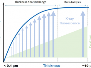
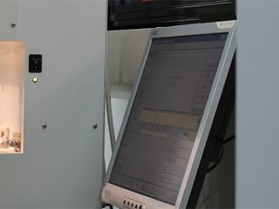
The thickness of metallic coatings is routinely determined by X-ray fluorescence spectrometry. This provides a basis for assessing the quality of coated materials and therefore influences decisions regarding disposition (acceptability) of coated product as well as control of...
The purpose of this test is to measure bond strengths, to evaluate bond strength distributions and to determine compliance with specified bond strength requirements of the applicable acquisition document in order to ensure the proper manufacturing process and long-term...

Burn-in test is an electrical stress test that employs voltage and temperature to accelerate the electrical failure of a device.

Destructive Physical Analysis, dpa , is a systematic, logical, detailed examination of EEE parts during various stages of physical disassembly. This activity is performed to verify that the manufacturing lot quality and construction are in accordance with the detailed...