Decapsulation of packaged devices exposes the internal elements of the device under test. Opening devices by this method allows the inspection of the die, interconnects and other features typically examined during failure analysis (FA), constructional analysis (CA) and destructive physical analysis (DPA).
Some preliminary steps should be performed before the decapsulation:
- X-ray analysis in order to determine the shape, placement and size of the die and the height of the bond wires. This information assists in choosing the correct mask or gasket and/or depth of the trench to be milled in the package surface.
- Plastics packaged samples should be baked before wet decapsulation. This step is intended to remove all moisture from the package so damage will not occur due to acidic corrosion of the metallization.
Device FA often relies on the selective etching of polymer encapsulants without compromising the integrity of the wire bonds and device layers. This is achieved by using the following techniques (in accordance with MIL-STD-883, MIL-STD-750, and MIL-STD-1580):
- Opening the lid manually using mechanical methods and performing the internal visual inspection. A quick result is possible with readily available equipment. Mechanical decapsulation offers key advantages for topside sample preparation (compared to chemical-etch and dry-decap), as well as for avoiding bond wires and thus optimizing the survivability of chemical-etch and dry-decap systems as it alows to avoid the inner part of the component being damaged by testing agents.
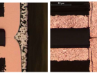
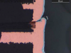
- Wet chemical jet etching. This method eliminates some safety problems inherent to manual wet etching and provides quick, clean, and localized removal of encapsulant in the die area, usually with no damage to the part. Using a proper technique to protect copper wires is necessary since not every jet etching equipment guarantees it.
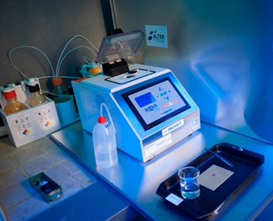
FIGURE. Wet chemical jet etching equipment.
- Plasma etching. The etching properties of the plasma are highly selective leaving interconnects and bond pads unaffected by the plasma etching process. This system alows to remove the glassivation layer which protects the metal paths of some semiconductor devices as well as to eliminate the plastic case. The plasma destroys certain materials leaving the others undamaged, thus facilitating a very precise analysis.
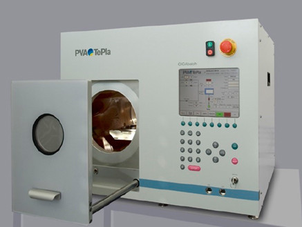
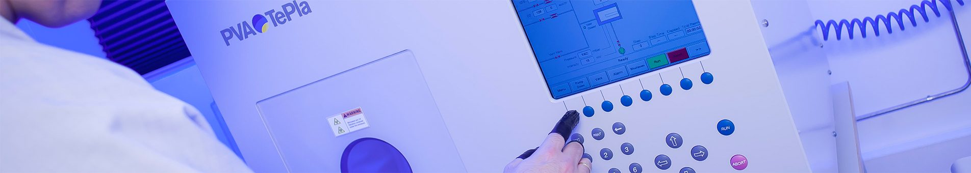
FIGURE. Plasma Giga-Batch

Degree in Physics and Ph.D. in Materials Science by the University of Seville.
Since 2007 Dr Aparicio has developed a productive research career within the field of Materials Science including post-doctoral stays at the University of Trento, the University of Mons, and the Spanish National Research Council (CSIC). His researches have been published in more than 30 articles in reputed international research journals and conferences (> 70) including more than 10 invited talks and lectures.
Within the frame of the programme “Torres Quevedo” for the Knowledge Transfer and the incorporation of research talent into the industry, in 2019 he joined Alter Technology as Senior Materials Science Test Engineer. In 2019 he was appointed to lead the Scanning Acoustic Microscopy Service. Within this framework, he currently collaborates in different ESA projects (JUICE and PLATO).”
Latest posts by Francisco Javier Aparicio Rebollo (see all)
- Scanning Acoustic Microscopy on Ceramic Capacitors - 18th May 2020
- Non-destructive detection of micrometric internal features within EEE microelectronic systems. - 3rd September 2019
- Acoustic Inspection of Hybrid Systems on Laminated Substrates - 3rd September 2019