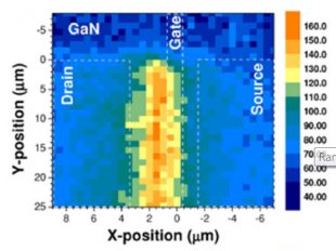
Raman thermometry is a thermal characterization technique which makes use of Raman scattering phenomena to determine the local temperature in microelectronics systems. Non-contact character. High spatial resolution (sub-micron scale). In-depth analysis within IR-transparent... Continue reading
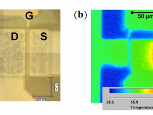
IR thermal microscopy (or infrared radiation thermometry) analyses the spatial distribution of the emitted infrared radiation either over the device surface or eventually inside the inspected device. This technique enables us to obtain 2D temperature maps, which are used to... Continue reading
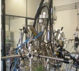
X-ray photoemission spectroscopy (XPS) also known as electron spectroscopy for chemical analysis (ESCA) is a surface-sensitive quantitative analysis method to accurately determine the elemental composition of solid materials. The technique is the most extended tool for the... Continue reading

XRF is a non-destructive and quick analytical tool to determine the chemical elements present in the specimen. In particular, it combines low detection limit (particularly in the case of heavy elements) with quick and easy sample preparation. Continue reading

The new century brought to the space a new type of solar cells with higher efficiencies and better resistance to radiation damage such as those based on the III-V single-junction GaAs. This new material opened the possibility of further improvement by the development of the... Continue reading
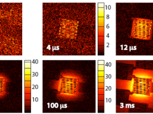
Submicrometric-nanometric objects nowadays present in the design of integrated circuits induce singular heat transport phenomena leading to the formation of hot-spots or strong temperature gradients at specific local points, which compromises the suitable operation and... Continue reading
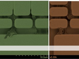
Surface contamination involving micrometric particles, microbiological agents, molecular adsorbate and others, represent a significant hazard in many areas of industry. For instance, a high level cleanliness is a critical requirement that any EEE device has to fulfil at any... Continue reading
Material Analysis is performed to detect and identify the materials used in the manufacturing of semiconductors and microelectronic parts and packages. One particular use of this analysis is the detection of prohibited materials, especially in the lead finish, to identify... Continue reading
The reliability of the components used in a spacecraft is a determinating factor for their operation and performance throughout the mission life. Only the most advanced techniques are able to provide the depth and accuracy in the inspections required by current state of the art... Continue reading
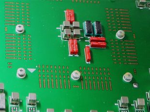
In-house capacity, capability and expertise to perform electrical screening of any type of electronic component technology. For passive devices testing, we have equipment which permits the characterization of the electrical behavior of resistors, capacitors, coils, etc., in a... Continue reading
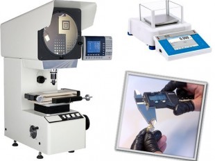
The purpose of the inspection is to detect: Manufacturer deviations Handling damages that could affect the device assembly and its final application Continue reading
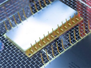
The purpose of this test is to verify that the markings on component parts will not become illegible when subjected to solvents (e.g. during the board cleaning process after parts assembly) or during normal handling, and that the solvents employed for the test will not cause... Continue reading

