Material Analysis
Material Analysis is performed to detect and identify the materials used in the manufacturing of semiconductors and microelectronic parts and packages. One particular use of this analysis is the detection of prohibited materials, especially in the lead finish, to identify potential reliability issues such as undesirable whisker growth caused by pure tin finishes. Lead finish validation for every component type to be soldered is essencial to determine the correct soldering profile.
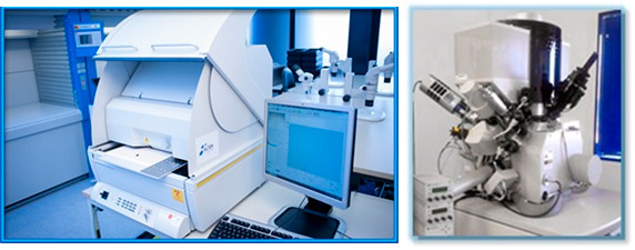
X-ray fluorescence equipment (XRF) is used to perform the material analysis. XRF allows to identify the metals present in complex samples while providing quantitative accuracy sufficient to preclude prohibited material or its inadequate proportions.
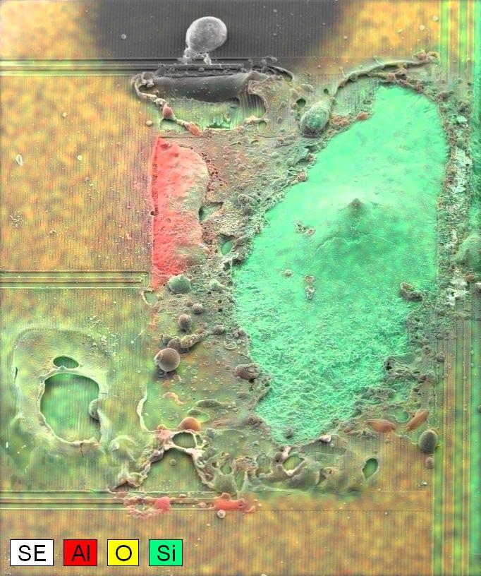
Scanning Electron Microscope (SEM) microanalysis can be performed through EDS (Energy Dispersive X-ray Spectrometry). This method allows to get information about the presence of elements (metals and non-metals) and their mass percentage in each area of the sample. The fact that the equipment is capable of detecting organic materials makes this method especially useful for discoloration analysis, which involves the examination of oxides content. However, as opposed to XRF, EDS is a destructive technique.
Material analysis is typically performed during the incoming inspection when scan locations for the analysis are selected depending on the specific requirements and the detailed specification of each part. It also may be implemented as a go/no-go test when specific requirements need to be checked, or may include read-and-record measurements and graphical analysis of the data obtained.
Advanced Techniques in Electrical, Electronic and Electro-mechanical (EEE) Components Testing. from Alter Technology on Vimeo.
- Inmunidad conducida - 20th mayo 2019
- Ensayos de Transitorios eléctricos - 2nd mayo 2019
- Ensayo Campo de RF radiado - 2nd mayo 2019