Wafer Sawing Process
Wafer Sawing is the process of singulating the wafer into individual die ready for subsequent assembly.
Alter Technology (formerly Optocap) has the capability for Wafer saw of substrates up to 8” diameter. When dicing of substrates of 12” diameter is required then Optocap can process 12” substrates into smaller segments prior to dicing.
For many System-in-Package (SiP) applications a very thin semiconductor die is required in order to meet the demanding package form factor requirements.
Our engineers have experience of mounting and dicing thin wafers down to 100um in thickness. Alter Technology UK can also offer Backgrind services and dice before Backgrind processes to singulate die down to as little as 50um thick. In addition to handling very thin die our company can also dice substrates up to 1mm thick.
We have an extensive experience in wafer dicing a wide variety of substrates including 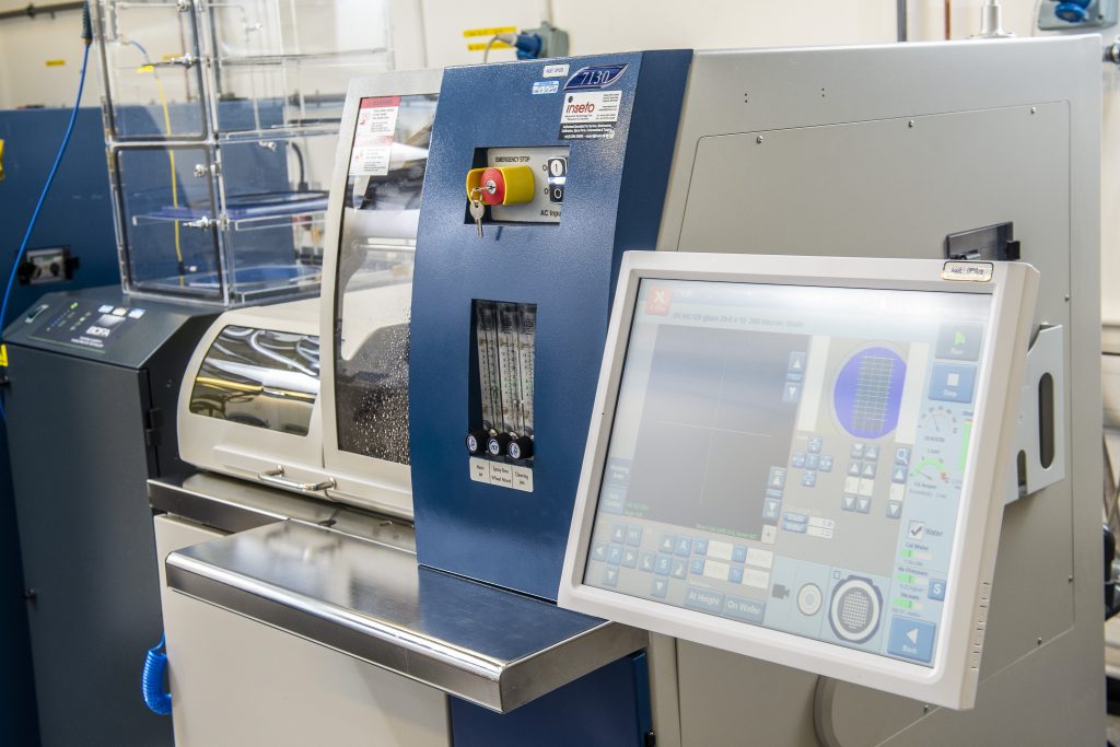 Si, Multi-Project Wafers (MPW), GaAs, GaN, FR4, Glass, Ceramics and Laminates. Different dicing blade thickness and materials are used depending on the substrate material and thickness.
Important parameters during wafer saw include feed speed, spindle rev, blade height, and water flow. Important parameters for the washing step include wash time, wash rpm, DI water pressure, dry time, dry rpm, temperature and airflow rate. As a company, we have developed a number of optimized wafer saw and wash processes for various MEMS and Sensor devices in order to avoid damage to the sensitive membrane and optical surfaces.
Alter Technology UK expertise and capability in wafer sawing will reduce risk and reduce time to market for your wafer saw requirements as well as providing a cost-effective manufacturing option.
Contact us for more information
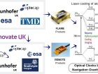
- Quantum Key Distribution - 7th November 2022
- Conducted Immunity - 20th May 2019
- Electrical transients Test - 2nd May 2019