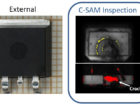
Internal (invisible) fabrication and materials defects can critically compromise the performance of encapsulated microelectronics parts. Similarly, accidental constructional failures (missing parts) and counterfeit suppose and non-negligible issue in the current EEE market. Therefore, reliable non-destructive inspection tools are essential for the for the suitable identification and screening of internal defect in encapsulated systems.
However, internal non-destructive inspection becomes a challenging task because of the higher complexity and miniaturizations of current EEE assemblies, for instance chip-scale packages and 3D integrated circuits stacks. In this regards Scanning Acoustic Microscopy (SAM) is one of preferred methods for the non-destructive inspection of microelectronic assemblies and components.
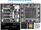
- Plastic encapsulated IC
- Flip Chip systems (CGA, FCBGA, PBGA, FPBGA…)
- Bonded Wafers
- Printed Circuit Boards
- Capacitors
- MEMS…
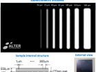
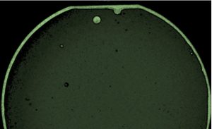
Amongst other types of failures acoustic techniques are particularly suitable for the detection of those irregularities involving materials and density changes including voids and porosity as well as cracks and delamination. In particular, acoustic microscopy has proved to be the ultimate non-destructive approach for the identification of ultrathin air delamination in multilayer systems, being sensitive to air features of sub-micrometric thickness. Therefore this non-destructive testing method is included in different quality control verification programmes such us:
- IPC/JEDEC J-STD-020E “Moisture Reflow Sensitivity Classification for Nonhermetic Surface Mount Devices”
- GEIA-STD-0006 “Requirements for Using Solder Dip to Replace the Finish on Electronic Piece Parts”
- MIL-STD-883 Test Method 2030 “Ultrasonic Inspection of die attach”
- MIL-STD-1580 “Destructive Physical Analysis for Electronic Electromagnetic and Electromechanical Parts”
- MIL-PRF-123 ”Capacitors Fixed Ceramic Dielectric (Temperature Stable and General Purpose), High Reliability, General Specification For”
- MIL-PRF-31033 “Capacitor Fixed Ceramic Dielectric High Reliability Discoidal General Specification For”
- MIL-PRF-49470 Capacitors, Fixed Ceramic Dielectric Switch Mode Power Supply (General Purpose and Temperature Stable) Standard Reliability and High Reliability, General Specification For
General failures:
- Non-bonded interfaces (e.g. bonded wafers)
- Die tilt or cupping
- Interlaminate disbonding
- Porous or insufficient die attach
- Die cracks
- Molding compound voids
- Chip package cracks
- Delamination within the substrate
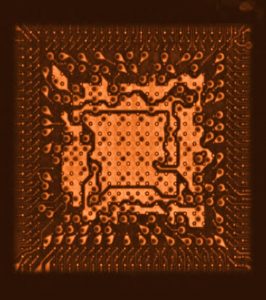
Ball Grill Arrays and specific failures.
- Defects in Cu pillars, solder balls and TSVs
- Excessive filler height or die attach material
- Solder mask or “lead finger” disbanding
- BGA package cracks
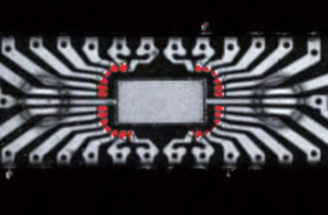
Integrated circuits specific failures
- IC package cracks (“popcorn” cracks)
- Lead frame delamination
Hybrid and Multi-Chip Module (MCM) specific failures
- Heat sink solder bond integrity
- Lid seal bond quality
- Insufficient solder material
- Excessive solder reflow
- Seal integrity
REAL TIME FEEDBACK
Our Vitual Lab Platform for Remote Testing provides Alter Technology users with:

- Instant access to test results
- Live chat with our inspectors during and after test duration
- Access to Alter Technology data base (30 years of accumulated data) for performance comparison with other batches and similar components.
Thanks to the Virtual Lab tool the customer can devise his own test solution specifically adapted to the actual needs and requirements and monitor test results in real time, without the need to wait for the completion of all the activities. Therefore, the final user can adapt the inspection areas and planes depending on the initial results. He will also receive feedback and advice from our test engineers during or thereupon inspection.
Detailed inspection records can be accessed immediately after the activity completion. Thus, manufacturers and users gain valuable time to develop contingency plans and solutions to address detected anomalies.

Since 2007 Dr Aparicio has developed a productive research career within the field of Materials Science including post-doctoral stays at the University of Trento, the University of Mons, and the Spanish National Research Council (CSIC). His researches have been published in more than 30 articles in reputed international research journals and conferences (> 70) including more than 10 invited talks and lectures.
Within the frame of the programme “Torres Quevedo” for the Knowledge Transfer and the incorporation of research talent into the industry, in 2019 he joined Alter Technology as Senior Materials Science Test Engineer. In 2019 he was appointed to lead the Scanning Acoustic Microscopy Service. Within this framework, he currently collaborates in different ESA projects (JUICE and PLATO).”
- Scanning Acoustic Microscopy on Ceramic Capacitors - 18th May 2020
- Non-destructive detection of micrometric internal features within EEE microelectronic systems. - 3rd September 2019
- Acoustic Inspection of Hybrid Systems on Laminated Substrates - 3rd September 2019