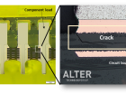
Manufacturing defects ascribed to improper fabrication.
Plating Thickness

Figure 1.From ECSS-Q-ST-70-60C Dir.1
The performance of a PCB systems are sensitive to variations in the plating thickness of its vias, depends on the current/time in the cooper plating bath and the throwing power. Insufficient plating thickness reduces the mechanical and thermal properties of the board and may lead to fatigue or overstress cracking, such us corner cracking and barrel cracking described below.
Suitable assessment of the plating thickness and integrity must be conducted by cross-sectional metallographic inspection, which allows us to measure the plating thickness at three depths as it is typically required by quality standards. The average of these measurements provides the nominal plating thickness which must meet the required specifications.
Plating Voids
Quality standards state a maximum void size in order to preclude plating-voids caused functional failures.Voids or non-plated areas are one of the most common deposition defects in PTV walls. Such defects are related to abrupt topographic irregularities on the walls of the hole that the plating process is not able to homogenously coat with a continuous and defect free layer. The initial roughness of the wall could be caused by contamination, air bubbles in the sides of the hole, and/or rough drilling.

Figure 2 From ECSS-Q-ST-70-60C Dir.1
Plating Nodules
Hole surface uniformity is sometimes disrupted with the presence of nodules, which could create highly stressed areas in the plating wall. These reduce lifetime when the PCB works under extremal environmental conditions.
The growth of these roughness elements could be related to poor drilling, surface contaminants (especially additive or organic particle contamination), elevated solution temperature, or excess brightener levels.

Figure 3 From ECSS-Q-ST-70-60C Dir.1
Etchback and Glass fiber protrusion
Etchback is the distance from resin of hole wall to innerlayer foil. It can be both positive or negative depending on the used processes. The possible causes of such anomaly are: high bath etching temperatures, elevated etching times or high etchant concentrations. Negative etchback has a tendency to cause foil cracks.
Glass fiber protrusion into PTH walls leads to poor plating distribution creating stress points and hence can contribute to PTH cracking. Glass fiber protrusion may be due to process control variabilities during hole drilling, hole preparation or plating deposition.

Figure 4 From ECSS-Q-ST-70-60C Dir.1
Corner Cracking
These cracks appear on the knee of the PTH. During manufacturing they are ascribed to poor plating caused by an excess of additive or organic contamination in solution.
When Corner cracks appear after thermal treatment the origin shall be attribute to: different CTE of the materials, high thermal excursions, and insufficient plating or poor plating quality.

Figure 5 From ECSS-Q-ST-70-60C Dir.1
Barrel crack
Most occurrences of barrel cracking tend to be governed by the presence of manufacturing defects. The main sources of cracks are etch pits, glass fiber protrusion, insufficient plating thickness, plating folds and voiding.
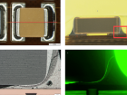
Microsection inspection.
Due to the buried architecture surface visual inspection only provides limited information about the actual status of PTV. Therefore, comprehensive analysis can only be accomplished by combining cross-sectioning and metallographic techniques.
Micro-sectioning is a delicate destructive process whereby the PCB area under inspection or a test coupon is precisely excised from the system to be mounted in an epoxy resin. Afterwards the sample is ground and polished according to the system characteristics in order to reveal the true internal structure. This is a complex task involving different preparation steps adapted to the sample characteristics that require highly trained staff, to avoid preparation induced anomalies.
In contrast with to other labs in Alter Technology combine micro section inspection with fluorescence microscopy techniques, which has been proved to be an effective approach to avoid false rejections and to highlight small anomalies.
In Alter Technology micro-sectioning is accomplished in a specifically dedicated laboratory and by ESA certified staff on PCB/SMD inspection. ESA selects those laboratories that according to the higher quality standards are recommended to perform such operations on SMT/PCB systems. It is worth mentioning here that due to the high-level standard that Alter Technology maintains in all its activities it is currently an ESA recommended laboratory to conduct metallographic inspections in SMT systems.
Contact us for more information

She is responsible for the Materials & Process Laboratory of Alter Technology. Her work is focused on investigating the effects of the environment on electrical components, materials, and processes. As the head of the laboratory, she also manages the studies conducted to evaluate the quality of a bare or assembled printed circuit board in relation to ECSS standards or according to the customer’s specifications.
- MacroVoids in assembled BGA packages - 14th August 2019
- Microsection Inspection / Constructional Analysis - 23rd July 2019
- Microsection Inspection / Failure Analysis - 19th July 2019