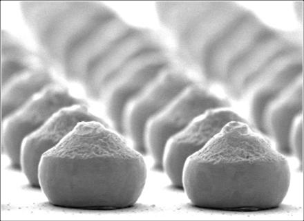
Alter Technology (formerly Optocap), has the ability to Gold (Au) stud bump wafers and individual die making them ready for a subsequent flip chip attach process
Stud Bumping
Gold stud bumping forms Au bumps using a process very similar to Au ball wire bonding. Like wire bonding it forms an Au ball (stud). However, the wire is terminated after the first bond so there is only a bump on the die.
Au stud bumping requires no Under Bump Metalization (UBM) or special wafer preparation, unlike the requirements for solder bumping. It also offers finer bump spacing than most solder bump technology without the added expense of a solder re-distribution layer.
Au stud bumps can be used on individual die or wafer and typically have much lower set-up costs than a solder bump approach. The ability to bump individual die makes Au stud bumping an extremely valuable tool in the prototyping phase, as well as a viable option for volume manufacturing.
For many sensitive devices such as lasers, MEMS and sensors the use of flux or adhesives is not allowed and a thermosonic or thermocompression Au-Au attach process offers a reliable flux free process to improve the device reliability.
Au stud bumps can be produced in wide variety of diameters and shapes depending on the application. For example, Stud bumps with diameters of 40-100um can be produced with heights of 20-80um. Co-planarity of +/-2.5um can be achieved without coining process. Stacked bumps can be used to increase the stand-off distance between the die and substrate to help accommodate substrate thickness variations and minimise CTE differentials. Gold stud bumps with pointed tips can be used for subsequent epoxy dipping.
Alter Technology UK expertise and capability in Gold Stud bumping will reduce risk and reduce time to market for your Gold stud bumping requirements as well as providing a cost-effective manufacturing option.
Contact us for more information
- Quantum Key Distribution - 7th November 2022
- Conducted Immunity - 20th May 2019
- Electrical transients Test - 2nd May 2019


