Flip chip
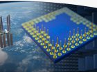
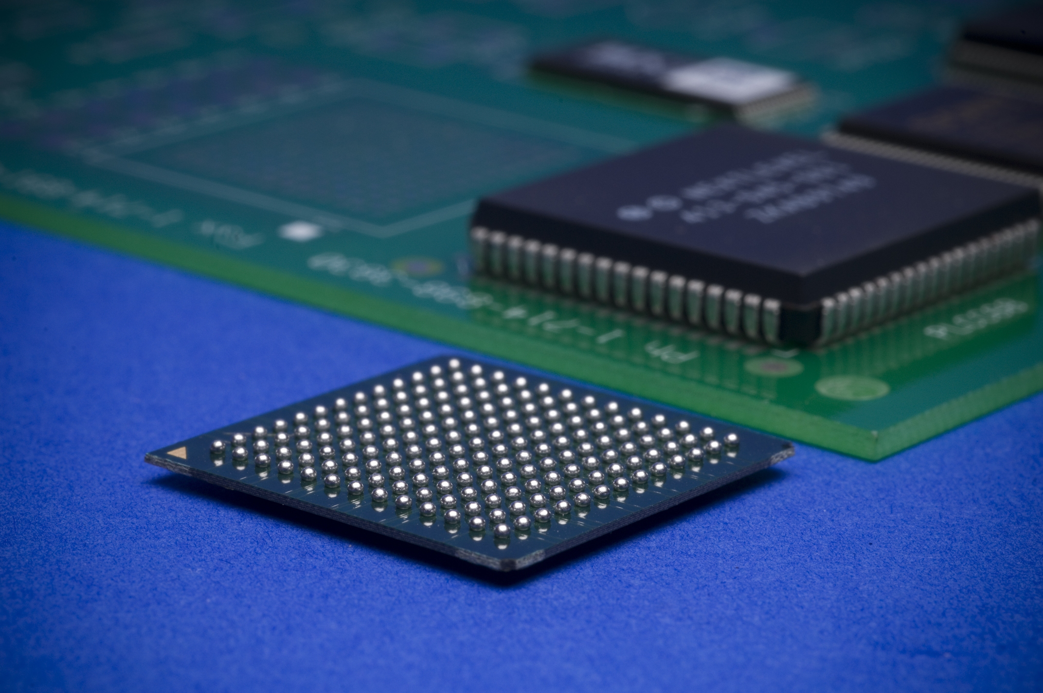
Flip chip (also known as direct chip attach) is the process whereby a semiconductor die is attached bond pad side down to a substrate or carrier. The electrical connection is made by means of a conductive bump on the die bond pad.
Once the die is connected the stand-off distance between the die and substrate is typically filled with a non-conductive adhesive referred to as underfill. The underfill provides stress relief between the die and carrier, provides robustness, and protects the component from any moisture ingress.
Flip chip bonding can offer a number of advantages over other interconnection processes. Flip chip bonding can provide higher I/O count as the whole area of the die can be used for connections. Due to the short inter-connection paths, compared to wire bonds, the speed of a device can be improved. In addition, as wire bonds loops are removed it provides a smaller form factor.
Alter Technology (formerly Optocap), has detailed know-how in a wide variety of processes and materials;
- Typical Materials
- Substrate: BT Laminate, Ceramic, FR4, silicon
- Packages: Customer specified
- Underfill: Hysol FP4530, FP4511, Fluxing Underfills etc.
- Bump material; Au stud bumps, Eutectic, High Pb, Pb free, Sn coated Au ball bumps.
- Die: Si, GaAs, GaN, SiGe, MEM’s, InP
- Attach Process
- Thermosonic or Thermocompression Au-Au attach
- Solder bump reflow processes
- Epoxy assisted processes on Au stud bumps
X-ray and cross-sections can be used to asses the interconnection joints and temperature cycling used to asses the reliability.
Alter Technology UK expertise and capability in flip-chip bonding will reduce risk and reduce time to market for your flip-chip bonding requirements as well as providing a cost-effective manufacturing option.
Contact us for more information
- Quantum Key Distribution - 7th November 2022
- Conducted Immunity - 20th May 2019
- Electrical transients Test - 2nd May 2019