There are well-known advantages to using these photonic technologies in space, such as the limited generation of noise, electromagnetic immunity,
A key function of an optoelectronic device is to manipulate light. As a result the packaging and assembly processes for many optoelectronic components can be significantly more complex than traditional microelectronic devices.
Surface contamination involving micrometric particles, microbiological agents, molecular adsorbate and others, represent a significant hazard in many areas of industry. For instance, a high level cleanliness is a critical requirement that any EEE device has to fulfil at any...
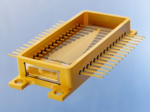
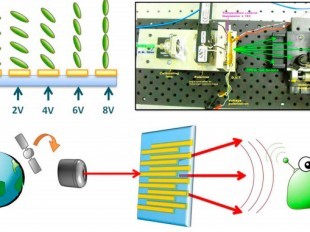
Passive liquid crystal (LC) devices are becoming an interesting alternative for the manufacturing of photonic devices in spatial applications. These devices feature a number of advantages in this environment, the lack of movable parts, and of exposed electronics being among the...
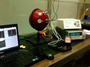
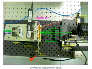
Clean area with a laminar flow chamber (class 100) Optical table with vibration stability ESD free area 1064 nm, 1310 nm and 1550 nm lasers with a modulation option of up to 20 GHz Integrating sphere (250 – 2500 nm) and detectors Spectrum analyser (600 – 1750 nm, resolution 20...
This article describes the setup developments and some of the results obtained for the temperature characterization from -190ºC to more than +300ºC of passive components normally used for space missions, but with a standard operating temperature range in most of the cases. One...
The use of photonic technologies for space applications has risen the problem related to the ability of optoelectronic and optic components to withstand space environment as all optoelectronic and optic components come from terrestrial applications. Therefore, the development of...
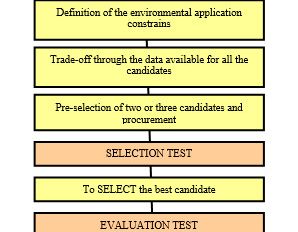
After expose key elements on the evaluation of Optoelectronic Components for Space Applications, where thermal vacuum and other environmental restrictions such temperature range, radiation or vibration and examples of Optoelectronic characterizati0ons done in our laboratories...
Conferences & Publications Innovation;
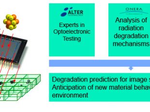
To study and predict radiation induced degradation of optoelectronic devices, with particular interest in image sensors based on APS (active pixel sensing) technology, as well as of InGaN, GaP and AlInGaP semiconductor materials.
Project developed in the frame of ESA TRP contract -Environmental characterization of different LC technologies -Design and manufacturing of EBB laser beam steering based on LC -Thermal, thermal vacuum, vibration and radiation tests
Examples of Projects: Radiative optoelectronic components vulnerability Britespace Photonic transceiver for secure space communications