Non-destructive testing methods are critical for the screening, inspection and failure analysis of plastic encapsulated and other EEE systems. Typical non-destructive testing activities involving EEE parts are grouped in three main categories:
- Functional inspection (electrical tests to find functional failures)
- External inspection of the package
- Internal inspection of the structure
The present post addresses and compares three differed non-destructive inspection methods used in Alter Technology for such activities.
- Acoustic Microscopy
- X-ray inspection
- Lock-in Infrared Thermography
These and other inspection methods are combined with other destructive and functional tests used for the detailed analysis and study of:
- Plastic encapsulated IC
- Flip Chip systems (CGA, FCBGA, PBGA, FPBGA…)
- Bonded Wafers
- Printed Circuit Boards
- Capacitors
- MEMS
Next figure shows the state of the start of each non-destructive inspection method in terms of spatial resolution and compared to typical sizes in the current IC packed technology according to a recent review published in Sensors (Sensors 2018, 18, 1981; doi:10.3390/s18071981).

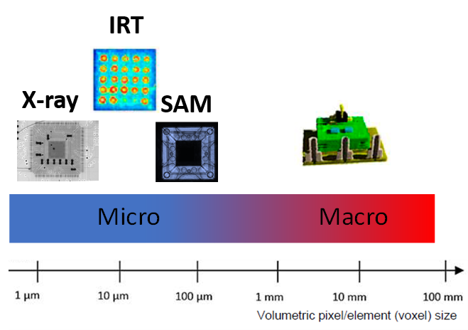
Figure 1. Non-destructive inspection tests vs spatial resolution adapted from “Sensors 2018, 18, 1981; doi:10.3390/s18071981”
X-Ray Inspection
When an X-ray beam propagates through the specimen a percentage of the X-ray photons interact with the media and are absorbed by the sample. Thus, the intensity of the transmitted X-ray beam depends on the elemental composition of the material and geometry of the specimen. Thus, internal features modify the intensity of X-ray beam registered at the receiver. Based on this mechanism the density and shape of internal objects can be measured and inspected by X-ray. Typical X-ray inspection systems consist of three components: X-ray tube (source), X-ray detector and test fixture used to fix and control the position of the sample in relation to the X-ray probe. In these systems the spatial resolution is mainly dictated by the size of the irradiation spot (focalization system) and the source emitting-area.
When an X-ray beam propagates through the specimen a percentage of the X-ray photons interact with the media and are absorbed by the sample. Thus, the intensity of the transmitted X-ray beam depends on the elemental composition of the material and geometry of the specimen. Thus, internal features modify the intensity of X-ray beam registered at the receiver. Based on this mechanism the density and shape of internal objects can be measured and inspected by X-ray. Typical X-ray inspection systems consist of three components: X-ray tube (source), X-ray detector and test fixture used to fix and control the position of the sample in relation to the X-ray probe. In these systems the spatial resolution is mainly dictated by the size of the irradiation spot (focalization system) and the source emitting-area.
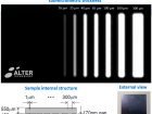
2D X-ray inspection is one of the oldest and more consolidated methods for non-destructive internal inspection of not only EEE parts but also raw materials. As it is illustrated in Figure 2, which compares X-ray inspection with CSAM microscopy, one of the main advantage of this technique relies on the capability to pass through thick objects and to detect sub-millimetric vertical features by recording top-down views of the samples However such planar views (Figure 3 right) do not provide enough information about internal structure of complex 3D assemblies and 3D reconstruction techniques are becoming a useful tool for the comprehensive inspection of such systems (Figure 3 right).
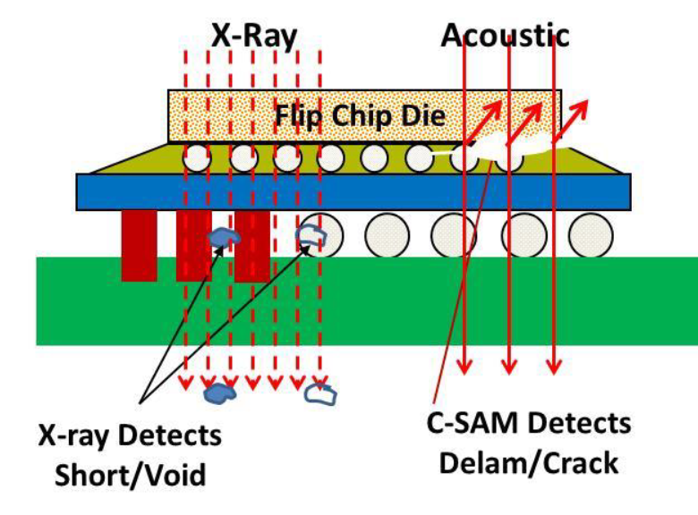
Figure 2. X-ray vs Acoustic Microscopy reprinted from “ECS Transactions, 33 (4) 47-57 (2010)”
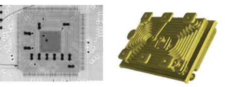
Figure 3. 2D (left) and 3D (right) X-ray non verification
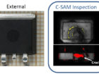
Scanning Acoustic Microscopy (C-SAM)
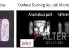
Scanning acoustic microscopy (SAM), also known as acoustic micro imaging (AMI) and scanning acoustic tomography (SAT), is currently a worldwide accepted technique for non-destructive verification, and inspection of microelectronic components and materials. It is commonly used for quality control, screening tasks and failure analysis as well as within DPA test flows, for instance in the case of plastic encapsulated integrated circuits (see Figure 4).
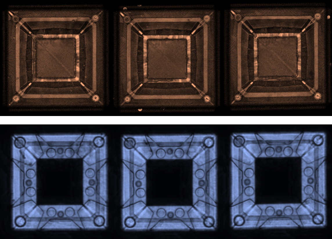
Figure 4. top and bottom C-SAM assessment of FPGAs
As it is illustrated in Figure 5, the working concept of the technique is based on the reflection that acoustic waves experience at the interface between different media and density irregularities, more information about the physics principles and instrumentation here (link to post How it works). Thus, the approach makes use of focalized ultrasound (MHz to GHz) pulses to image material interfaces and boundaries as well as hidden physical damages (voids, cracks, delamination, and others), either generated during manufacturing or induced after environmental testing or prolonged operation. The most important part of an acoustic microscope is the transducer, which is used as both source and receptor for acoustic to electrical signal conversion.
In this technique the delay between the reflected pulses generated at different interfaces the relative intensities are analysed for the reconstruction and inspection of the internal topography. In addition, it also provides very relevant information about other interface characteristics. Thereby, strong reflections (high reflection amplitude) are due to a high contrast between the materials properties, being material to air contrast the one providing more intense echoes as illustrates in Figure 5. Therefore, the technique is particularly suitable for the detection of ultrathin planar air features such as delaminations.
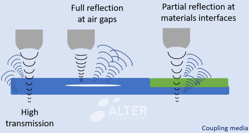
Figure 5. Physic principle of non-destructive C-SAM inspection
Lock-in Thermography
Infrared thermography (IRT) is also amongst the most commonly used non-destructive tests and inspection methods either for EEE components and materials evaluation. In this technique the heat luminance from the surface is accurately measured within the infrared electromagnetic spectral region (2–14 μm). As in the case of other thermal microscopy techniques such precise measurements are used to analyse and record the temperature distribution of the surface but with a resolution than can reach the 0.020 ◦C to 0.075 ◦C range depending on the used detector.
Either active or passive thermography techniques are used for the inspection of microelectronic as well as passive components. On the one hand passive methods analyse the natural thermal emittance from the different structures within the components without an external stimulus. On the other hand, active methods apply external heat to the inspected system by optical, mechanical or electromagnetic heat sources. Therefore, thermal waves are generated on the surface of the specimen, and these will be scatted at surface defects and subsequently detected. Active thermography methods are used in the detection of delamination and moisture in composites and for the inspection of high-density IC packages.
Pulsed and lock-in approaches are the main active-thermography techniques. In the case of pulsed thermography, a single heating pulse is used; whereas in the lock-in counterpart, the sample surface is periodically heated. In the latter cases when the heat wave reaches a thermophysical inhomogeneity (e.g., delaminations or inclusions), the input wave is reflected and modifies the surface temperature distribution. As the reflected wave oscillates at the same frequency as the excitation wave, it can be easily identified.

Figure 6. Lock-in thermographic inspection of connectors
Stress test
In Alter Technology these non-destructive inspection techniques are combined with different stress and environmental tests to analyse the effect on the system integrity and performance
- Humidity, moisture and thermal test.
- Thermal-vacuum testing
- Temperature cycling
- Thermal shock
- Vibration testing
Contact our team

Since 2007 Dr Aparicio has developed a productive research career within the field of Materials Science including post-doctoral stays at the University of Trento, the University of Mons, and the Spanish National Research Council (CSIC). His researches have been published in more than 30 articles in reputed international research journals and conferences (> 70) including more than 10 invited talks and lectures.
Within the frame of the programme “Torres Quevedo” for the Knowledge Transfer and the incorporation of research talent into the industry, in 2019 he joined Alter Technology as Senior Materials Science Test Engineer. In 2019 he was appointed to lead the Scanning Acoustic Microscopy Service. Within this framework, he currently collaborates in different ESA projects (JUICE and PLATO).”
- Scanning Acoustic Microscopy on Ceramic Capacitors - 18th May 2020
- Non-destructive detection of micrometric internal features within EEE microelectronic systems. - 3rd September 2019
- Acoustic Inspection of Hybrid Systems on Laminated Substrates - 3rd September 2019