Why Microsectioning sample preparation?
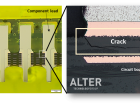
Microsectioning sample preparation is an essential tool for the detailed materialographic inspection of EEE parts, including solder joints on PCB systems involving both surface mounting technology (SMT) and through-hole technology (THT). In reveals critical information regarding the structural characteristics and the workmanship quality that is not accessible by other techniques. To illustrate this concept the figure shows several anomalies detected in a PCB that apparently did not present any deviation.
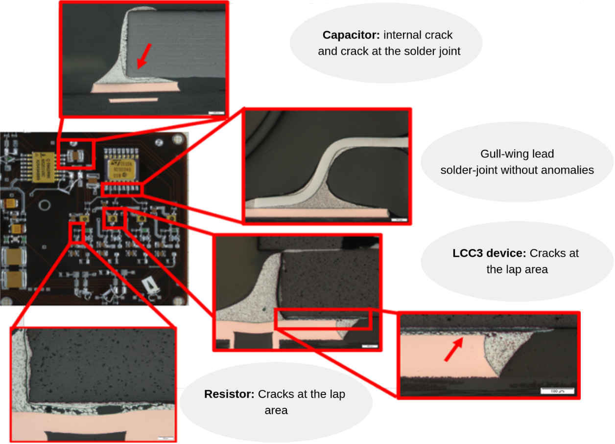
Anomalies detected in a PCB that apparently did not present any deviation.
Microsectioning and materialographic inspection are mandatory in different verification and qualification standards issued or adopted by international agencies and public bodies such as the European Space Agency (ESA), the Defense and Logistics Agency (MIL DLA specifications) and the IPC Association Connecting Electronics Industries.
Table: International specification requiring and/or describing microsectioning sample preparation.
| wdt_ID | Organization | Specification | Reference | Link |
|---|---|---|---|---|
| 1 | ECSS - European Cooperation for Space Standardization | Verification and approval of automatic machine wave soldering | ECSS-Q-ST-70-07C | http://ecss.nl/standard/ecss-q-st-70-07c-verification-and-approval-of-automatic-machine-wave-soldering/ |
| 2 | ECSS - European Cooperation for Space Standardization | Manual soldering of high-reliability electrical connections | ECSS-Q-ST-70-08C | http://ecss.nl/standard/ecss-q-st-70-08c-manual-soldering-of-high-reliability-electrical-connections/ |
| 3 | ECSS - European Cooperation for Space Standardization | Qualification of printed circuit boards | ECSS-Q-ST-70-10C | http://ecss.nl/standard/ecss-q-st-70-10c-qualification-of-printed-circuit-boards/ |
| 4 | ECSS - European Cooperation for Space Standardization | High-reliability soldering for surface-mount and mixed technology | ECSS-QST-70-38C-Rev.1 | http://ecss.nl/standard/ecss-q-st-70-38c-rev-1-15-september-2017/ |
| 5 | DLA - Defense and Logistics Agency (DLA) | Printed wiring board, flexible or rigid-flex General specification for | MIL-P-50884D | https://landandmaritimeapps.dla.mil/Downloads/MilSpec/Docs/MIL-PRF-50884/prf50884.pdf |
| 6 | IPC association connecting Electronics industries | Microsectioning Manual Method | IPC-TM-650 | https://www.ipc.org/TM/2.1.1E.pdf |
| Organization | Specification | Reference | Link |
Microsectioning sample preparation is a complex process that involves several preparation stages and each of them has to be specifically adapted to the design, materials and fabrication technology of the inspected electronic device.
In particular, special attention must be paid to the materials conforming the specimen since a wrong microsectioning protocol can induce spurious features, artifacts and even irreversible damage the sample. Hence, the present post focuses on the working methodology employed to study the status of solder connections in PCBs. Nonetheless, adapted approaches are successfully used in our laboratory to assess solder-less systems (Qualification of press-fit connector for space-flight applications, feedback and Design Improvements, F. J. Aparicio et al., SPCD 2018).
Accurate excision.
Firstly, the devices of interest have to be excised from the surrounding area by means of a precision diamond saw. During this operation, it is mandatory to maintain the traceability of each device in order to link the results with the corresponding soldered area.
Sawing is also used to adjust the sample size prior to encapsulation. The condition of such process is critical since depending on the removal speed, force, cooling system… it may add harmful stress to the PCB.
Low-temperature specimen Mounting.
 After that, the specimen is embedded in a resin mold to facilitate the handling during the following operations. This mounting process creates a flat surface, provides good edge retention and prevents additional damage during grinding. To obtain a good amount the resin should not physically or chemically damage the sample and should present a milar abrasion rate. Epoxy resins are the best choice since they fulfil the above requirements and are compatible with vacuum impregnation.
On the other hand, cold mounting processes are highly recommended to preserve the specimen integrity as they reduce both the thermal and mechanical stress exerted over the device under study. Unfortunately, such low exothermic processes involve longer cure time (typically of 8-12 h) in comparison to hot mounting resins, which are harmful to EEE system.
In contrast with other laboratories, in Alter Technology the mounting resin is systematically doped with a fluorescent dye. This approach is used to clearly detect and quantify by fluorescence techniques any crack and anomalies that otherwise would be omitted by conventional microscopy inspection.
Moreover, this systematic precaution allows us to unambiguously distinguish true anomalies from other features that rarely might be induced during the subsequent grinding and polishing. Note that this precaution minimizes the risk of false rejection inherent the sample preparation process.
Delicate polishing to reveal the “true surface”.
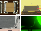
In the final step, a plane and polished surface with  few or negligible artefacts is produced to evaluate the status of the soldered connections of the devices. This is a multistage process as illustrated in the images, that combines several grinding and polishing operations.
The choice of the methodology and the grinding/polishing parameters (abrasive surfaces, speed, applied force, lubricants…) have a decisive impact on the quality of the final surface finish. They are selected to disclose the “true” internal structure (final Polishing image), i.e a high equality surface free of artefacts such as deformation, stretches, pull-outs and other features related to improper microsection processes. This requires adapting grinding and polishing steps to the design and materials of the inspected device.
To determine the relationship between grinding/polishing parameters and the quality of the surface finish, a Design of Experiments (DOE) method has been a powerful tool. This methodology together with the accumulated experience and the scientific background of our team enabled us to identify the main variables controlling the sectioning process, a knowledge that is used to predict the results, ensure replicability and minimize the processing time. These developments were presented in EMPS workshop organized by ESA in 2018. (Evaluation of Microsection Techniques for Materialographic Analysis of Electronic Devices, C. López-López et al., EMPS-9, 2018.).
Summarizing, at the begging of the process, planar grinding is used to quickly remove large amounts of material. Afterwards, abrasive silicon carbide (SiC) and diamond-coated surfaces are used in different stages depending on the material and size of the interesting device.
Finally, our experienced technicians use a carefully refined polishing process to yield a smooth finish, which is then ready for optical and fluorescence microscopy analysis.
Our commitment to quality
As it was mentioned before a wrong microsectioning protocol can induce spurious features, artefact and even irreversible damage the sample. The former may lead to a sleading interpretation of the actual quality of the device/solder joint or inspected device. Being this a critical issue that does not only depends on the used protocol but also on the skills and training of the technical team conducting the activities, the European Space Agency (ESA) selects those laboratories that according to the higher quality standards are recommended to perform such operations.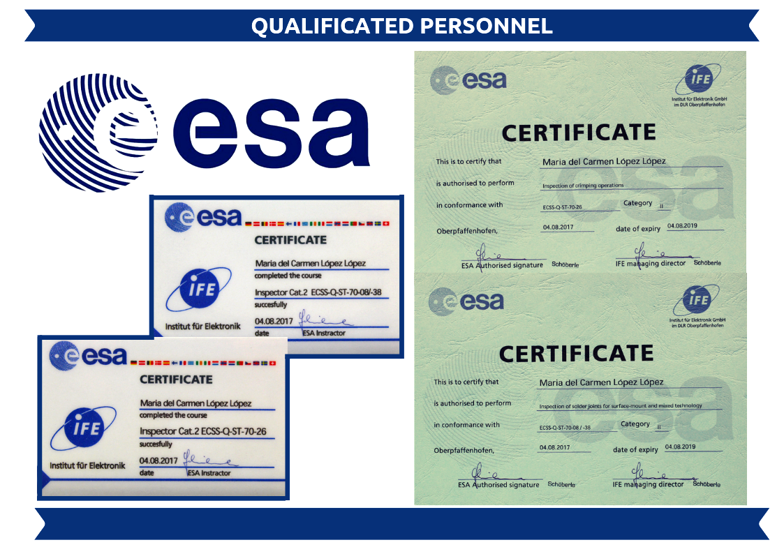
During this process, SA strictly reviews all the lab activities involved is these tasks, as well as those vibration and temperature cycling capabilities required for the verification of PCB systems according to toe ECSS-Q-ST-70-08C and ECSS-Q-ST-70-38C specifications.
It is worth mentioning here that due to the high-level standard that Alter Technology maintains in all its activities it is currently an ESA recommended laboratory to conduct this kind of inspections.

She is responsible for the Materials & Process Laboratory of Alter Technology. Her work is focused on investigating the effects of the environment on electrical components, materials, and processes. As the head of the laboratory, she also manages the studies conducted to evaluate the quality of a bare or assembled printed circuit board in relation to ECSS standards or according to the customer’s specifications.
- MacroVoids in assembled BGA packages - 14th August 2019
- Microsection Inspection / Constructional Analysis - 23rd July 2019
- Microsection Inspection / Failure Analysis - 19th July 2019