Material Analysis is performed to detect and identify the materials used in the manufacturing of semiconductors and microelectronic parts and packages. One particular use of this analysis is the detection of prohibited materials, especially in the lead finish, to identify... Continue reading
The purpose of the inspection is to detect: Manufacturer deviations Handling damages that could affect the device assembly and its final application Continue reading
The purpose of this test is to verify that the markings on component parts will not become illegible when subjected to solvents (e.g. during the board cleaning process after parts assembly) or during normal handling, and that the solvents employed for the test will not cause... Continue reading
PIND ( Particle Impact Noise Detection Test ) testing is performed in order to detect the presence of loose particles inside a device cavity. Loose particle contamination is often caused by dirt, fibers, solder residues and other elements trapped inside the cavity during the... Continue reading
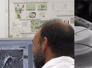
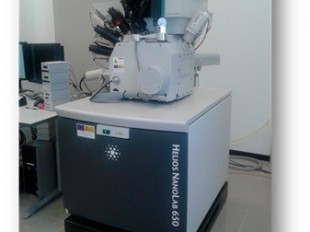
This type of inspection is performed using an electron microscope which produces images of a sample by scanning it with a focused electron beam. Interaction between the electrons and atoms in the sample generates signals that contain information about the sample’s surface... Continue reading
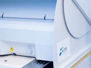
The purpose of radiographic inspection is to detect internal physical defects which are not otherwise visible in electronic components. The radiographic techniques reveal such flaws as presence of foreign objects, improper interconnecting wires, inhomogeneities in materials... Continue reading
Residual Gas Analysis, also known as Internal Gas Analysis (IGA), is a destructive test which is performed to examine the atmosphere inside hermetically sealed devices. The test procedure is based on milling the component so that the gas content can be extracted and subsequently... Continue reading
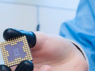
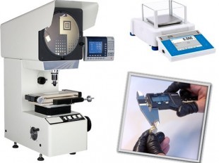
The aim of this process is to verify the conformity of the exterior of electrical, electronic and electromechanical components (EEE parts) with the acquisition document. The following aspects should be considered: Marking Aspect of Materials Workmanship Sealing Leads Feedthroughs Continue reading
This analytic technique may provide both qualitative and quantitative information of the composition of a surface, i.e. identification of the elements and the element weights, respectively. The technique relies on the detection and spectroscopy of secondary radiation (X-Ray)... Continue reading
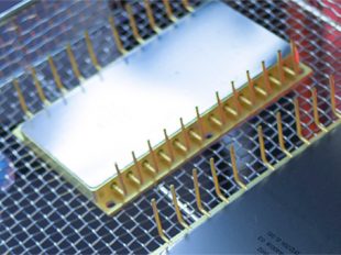
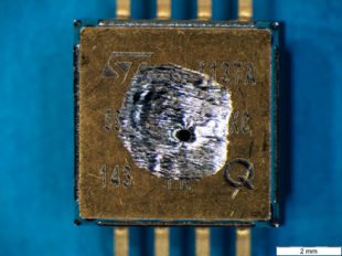
The aim of this destructive test is to demonstrate that the internal materials, design, construction and assembly of EEE parts are in accordance with the applicable acquisition document. This test can also be performed to examine unsealed devices prior to capping to verify that... Continue reading

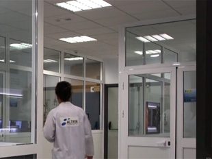
Receiving Inspection is an acceptance activity aimed at confirming that the components received are in accordance with the requirements of the applicable purchase order. Our inspectors verify all raw materials by reconciling the purchase order requirements with the packing slip... Continue reading

The purpose of the test is to determine the strength of the element attachment system when subjected to force in the Y1 axis, and thus to determine the integrity of materials and processes used to attach semiconductor die or surface mounted elements to package headers or other... Continue reading