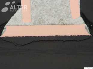
Pad Cratering One of the major failure modes encountered in PCB assembly is Pad cratering. This term is coined to describe a fracture at the pad/resin interface (adhesive failure) or within the resin beneath pads (cohesive failure) that extend along the whole pad length (see the... Continue reading

XRF is a non-destructive and quick analytical tool to determine the chemical elements present in the specimen. In particular, it combines low detection limit (particularly in the case of heavy elements) with quick and easy sample preparation. Continue reading
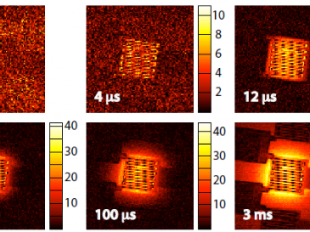
Submicrometric-nanometric objects nowadays present in the design of integrated circuits induce singular heat transport phenomena leading to the formation of hot-spots or strong temperature gradients at specific local points, which compromises the suitable operation and... Continue reading
Material Analysis is performed to detect and identify the materials used in the manufacturing of semiconductors and microelectronic parts and packages. One particular use of this analysis is the detection of prohibited materials, especially in the lead finish, to identify... Continue reading
The purpose of this test is to verify that the markings on component parts will not become illegible when subjected to solvents (e.g. during the board cleaning process after parts assembly) or during normal handling, and that the solvents employed for the test will not cause... Continue reading
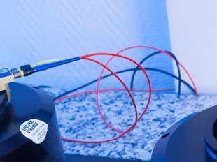
PIND ( Particle Impact Noise Detection Test ) testing is performed in order to detect the presence of loose particles inside a device cavity. Loose particle contamination is often caused by dirt, fibers, solder residues and other elements trapped inside the cavity during the... Continue reading
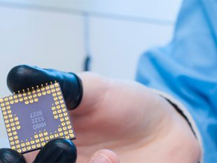
The aim of this process is to verify the conformity of the exterior of electrical, electronic and electromechanical components (EEE parts) with the acquisition document. The following aspects should be considered: Marking Aspect of Materials Workmanship Sealing Leads Feedthroughs Continue reading
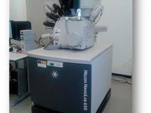
This analytic technique may provide both qualitative and quantitative information of the composition of a surface, i.e. identification of the elements and the element weights, respectively. The technique relies on the detection and spectroscopy of secondary radiation (X-Ray)... Continue reading

The aim of this destructive test is to demonstrate that the internal materials, design, construction and assembly of EEE parts are in accordance with the applicable acquisition document. This test can also be performed to examine unsealed devices prior to capping to verify that... Continue reading

The purpose of the test is to determine the strength of the element attachment system when subjected to force in the Y1 axis, and thus to determine the integrity of materials and processes used to attach semiconductor die or surface mounted elements to package headers or other... Continue reading
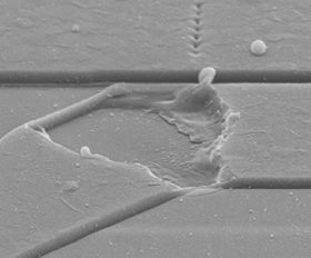
This test is performed to verify the structural quality of the glassivation layer in aluminium metallized semiconductor devices or microcircuits. The glassivation layer is a deposited dielectric film (e.g., CVD, sputtered of electron beam evaporated glass or nitride, etc.) and... Continue reading
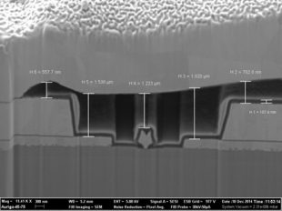
Focused ion beam, also known as ion milling, is a technique used particularly in the semiconductor industry and materials science for site-specific analysis, deposition and ablation of materials. Since it is destructive to the part, FIB technology is used for micro-sectioning in... Continue reading

