Pad Cratering
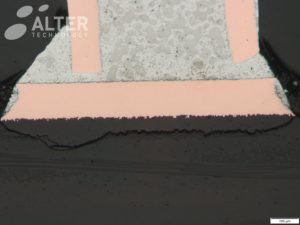
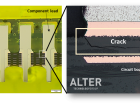
One of the major failure modes encountered in PCB assembly is Pad cratering. This term is coined to describe a fracture at the pad/resin interface (adhesive failure) or within the resin beneath pads (cohesive failure) that extend along the whole pad length (see the figure) and leads to the complete separation of the pad from the PCB. This failure mode is especially relevant for assembled BGA, CGA and bottom termination components fabricated by lead-free and halogen free processes and it is related to mechanical stresses experienced in PCB systems.
Though at the laboratory pad cratering is commonly detected after shock and other mechanical stress test failure may also be ascribed to thermomechanical stresses responsible for other types of damages in PTV systems.
First sings of Pad cratering appear as fine cracks typically observed after the manufacturing process. As the pad/PCB interface is submitted to mechanical or thermal stress the cracks grow until the pad is completely separated from the PCB resin and a pad “crater” is formed. Devices affected by pad cratering may not functionally fail in an early stage, however initial cracks may propagate into a copper trace or conduction pad, which results in permanent or intermittent electrical open. Therefore, an understanding of how this failure mode is produced is mandatory for improving PCB reliability in the long-term.
The main contributing factors include PCB thickness, size, resin type, CTE of the PCB and component, solder type, component position, assembly condition and post assembly handling. There are some strategies to mitigate the appearance of Pad Cratering failure, such as:
- Epoxy fillets at devices corners
- Increase board thickness to eliminate flexing
- Increase pad or trace widths
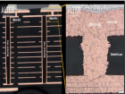
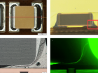
Since the initiation of pad cratering does not result in an instantaneous electrical signature, detecting the onset of this failure has been challenging. For instance units with pad cratering may not fail during functional test and Microsectioning Analysis remains the most widely accepted means for analyzing the Pad integrity.
Contributing Author: Francisco Javier Aparicio Rebollo
Contact us for more information
- MacroVoids in assembled BGA packages - 14th August 2019
- Microsection Inspection / Constructional Analysis - 23rd July 2019
- Microsection Inspection / Failure Analysis - 19th July 2019


