Physical Analysis and Materials
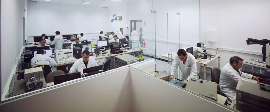
It is well known the negative effect that radiation can induce on electronic components and systems. There is a wide variety of effects that depend on the radiation environment (type of radiation: gamma, protons, cosmic rays …) and the type of technology and devices used. In this section we work to develop better tools to perform radiation tests, we will perform tests to understand and characterize the radiation phenomena on different technologies, exploring simulation tools and developing mitigation techniques to improve the radiation tolerance of different instruments electronic.
The new products offer better benefits: reduced sizes, greater speed, greater capacities, etc … The activity is dominated mainly by the consumer market: automotive, telecommunications, etc …, with products with a life cycle more and more short.
The changes are not only affecting the use of new semiconductor materials: SiC, GaN, …, new technologies: FinFet, …, and smaller dimensions (in the range of nanometers), …, but also to manufacturing processes, and the activities of encapsulation and integration, being necessary the accomplishment of meticulous analyzes that allow to characterize them.
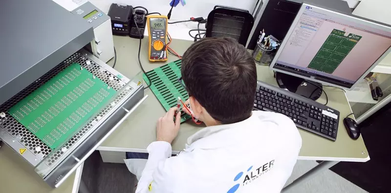
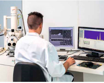
Under this framework we will develop a wide range of studies and tests (failure analysis, constructive analysis, evaluation tests, …, etc.) aimed at gaining confidence in these new products, so that we can consider their use in highly reliable applications. The investigations will be carried out using state-of-the-art inspection techniques such as FIB, AFM, TEM / SEM, dynamic X-ray and tomography, …, etc., also exploring new techniques and inspection methods that can contribute value to the process.
- Quantum Key Distribution - 7th November 2022
- Conducted Immunity - 20th May 2019
- Electrical transients Test - 2nd May 2019