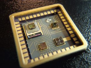
Alter Technology (formerly Optocap) has experience in the assembly and packaging of MEMS devices. Alter Technology (formerly Optocap) offers customers support in both prototype/process development for LED packaging as well as volume manufacturing capability. By prototyping on... Continue reading
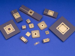
Alter Technology (formerly Optocap), is a leader in the design, manufacture and test of High Reliability Micro and Optoelectronics modules for Harsh Environments. We have experience in a number of high reliability and harsh environment markets such as Aerospace & Defence, Space... Continue reading
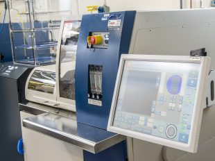
Wafer Sawing is the process of singulating the wafer into individual die ready for subsequent assembly. Optocap has the capability for Wafer saw of substrates up to 8” diameter. When dicing of substrates of 12” diameter is required then Optocap can process 12” substrates into... Continue reading
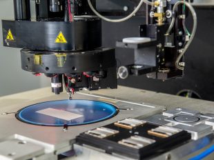
Pick and Place Alter Technology (formerly Optocap), has the capability to pick and place die from a variety of presentation formats with placement accuracies ranging from 1um to 15um. Die can be automatically picked from Gel-Pak, Waffle Pack and Wafer Film frame onto substrates... Continue reading
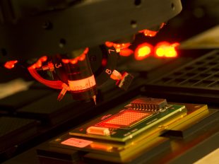
Die Bonding Services Die bonding is the process of attaching a die to substrate/package. Selection of the optimal die attach material and process is based on a number of issues including thermal requirements, electrical requirements and mechanical stability. Continue reading
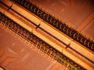
Wire bonding is the main method of making interconnections between a semiconductor die and a package or substrate. Optocap works closely with our customers at the package design stage to ensure that design for manufacturing techniques are applied and wire bond design rules... Continue reading
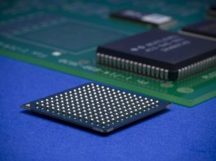
Flip chip (also known as direct chip attach) is the process whereby a semiconductor die is attached bond pad side down to a substrate or carrier. The electrical connection is made by means of a conductive bump on the die bond pad. Continue reading
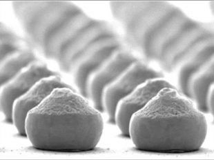
Au stud bumping requires no Under Bump Metalization (UBM) or special wafer preparation, unlike the requirements for solder bumping. It also offers finer bump spacing than most solder bump technology without the added expense of a solder re-distribution layer. Continue reading
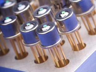
Optocap’s expertise and capability in Encapsulation and Hermetic Sealing will reduce risk and reduce time to market as well as providing a cost-effective manufacturing option. Continue reading
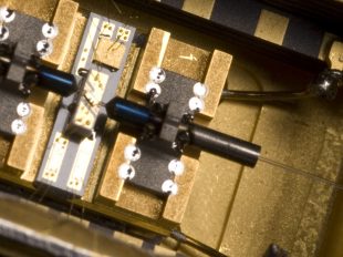
Optical Alignment by Optocap with an extensive experience in aligning and attaching fibers and optical components to wide range of optoelectronic devices including DFB lasers, Quantum Cascade lasers, SLEDs, SOA’s and Receivers. Continue reading
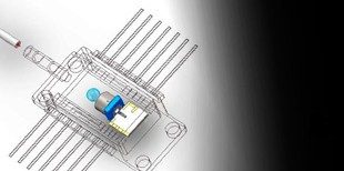
Our capabilities range from the simple selection of a ball lens for coupling the output of an optical fibre into a photodiode, to providing a much wider module design service. This may include proof-of-concept design evaluation, opto-mechanical and thermal tolerancing leading to... Continue reading
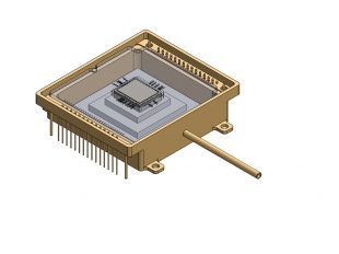
Package Design and Modelling Our company utilize Design for manufacturing techniques to ensure that any designs are compatible with a low cost, high yield assembly process. Optocap’s mechanical design experience covers custom hermetic packages, precision optical benches, heat... Continue reading

